


NVIDIA announced a new expanded NVIDIA NVLink Fusion architecture and unveiled a custom high-bandwidth memory technology called NVHBM. This technology integrates NVIDIA’s self-developed memory controller directly into the HBM base die, with Amazon’s Annapurna Labs becoming the first partner to adopt NVHBM in the next-generation Trainium4 chip. Compared with standard HBM4E, NVIDIA claims NVHBM delivers up to a 30% memory bandwidth improvement, a 15% reduction in HBM power consumption, and up to a 25% release of XPU compute die area.
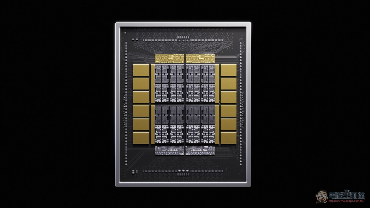
NVHBM is not new memory; it’s NVIDIA defining its own specification.
According to industry insiders.The analysis indicatesThe outside world can easily be misled by the name “NVHBM” into thinking NVIDIA has invented a new type of memory. In fact, the industry has long had a distinction between “standard HBM” (sHBM) and “custom HBM” (cHBM). cHBM has been in development for years, and NVHBM is just NVIDIA’s version of cHBM.
The core change in NVHBM is that NVIDIA defines the controller and interface specifications within the base chip itself, then has multiple memory suppliers produce to the same specification. The customized architecture that was previously co-designed by memory manufacturers and customers has now been moved entirely into NVIDIA’s platform layer.
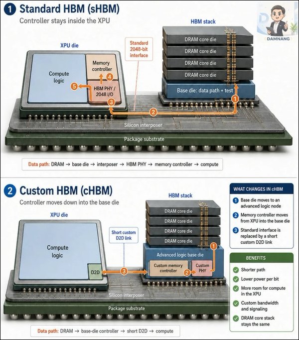
In the traditional cHBM model, memory vendors and customers co-design the base die architecture. Once a design is completed with one vendor, switching to another requires redesign and revalidation, and this switching cost is the core barrier protecting memory vendors’ custom design premium and customer relationships. NVHBM breaks this structure: NVIDIA defines the specification, multiple suppliers deliver to the same standard, and memory vendors’ differentiation space is compressed to yield, speed, power consumption, and manufacturing execution of the DRAM itself.
Counterpoint Research: The Trillion-Dollar Bottleneck Battle
Market research firm Counterpoint Research has framed the launch of NVHBM as a key step in the “trillion-dollar bottleneck” (The Trillion Bottleneck). Their analysis highlights several important aspects:
- NVHBM evolved from an architecture into a platform.From an architecture with only one customer (NVIDIA’s own GPUs), it has expanded into a platform with a channel. MediaTek has adopted NVLink Fusion and will promote it to its own XPU customers, backed by NVIDIA’s $3.5 billion (approximately NT$11.37 billion) investment.
- Broadcom bears the bruntNVIDIA can now directly sell chip architectures, rack designs, software, and memory subsystems into custom accelerator solutions without needing to build the accelerators itself. Marvell has joined NVLink Fusion, MediaTek is doing resale, and Broadcom has become the only major design firm not tied to NVIDIA.
- Memory control transfer:NVIDIA not only controls the interface from GPU to HBM, but also holds supplier selection power through a multi-source supply mechanism.
Why did HBM’s base chip suddenly become important?
Because HBM increases bandwidth by widening the interface between the XPU and HBM (from 1,024 bits in HBM3E to 2,048 bits in HBM4) and raising the signal rate. However, the issue is that a wider interface requires more PHY and I/O circuits on the XPU, taking up more chip area and interposer routing space.
On AI accelerators, this cost is especially heavy. The advanced-process chip area of XPUs is a precious resource and should be used as much as possible for compute and cache. The higher the HBM bandwidth, the greater the proportion of area and power consumed by the memory interface. The challenges beyond HBM4 require an architecture that achieves the same bandwidth with less XPU area and power.
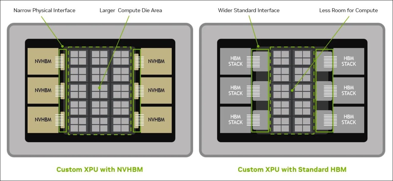
The cHBM approach moves part of the memory-related logic from the XPU onto a base die built on an advanced process node, redefining the interface from the XPU to HBM. This frees up area previously occupied by the HBM PHY and controller, returning the reclaimed silicon area and power budget to compute or cache. Micron has publicly stated that a customized HBM4E base logic die will bring higher gross margins than standard HBM4E.
NVIDIA’s bigger ambition: defining the entire AI system architecture.
NVHBM is just one piece of NVIDIA’s broader strategy, which aims to integrate compute, memory, and interconnect into a single AI factory architecture—HBM being only one component. Expanding outward from the GPU: NVLink and NVSwitch handle Scale-Up, Spectrum-X and InfiniBand handle Scale-Out, and with BlueField-4’s Scale-In and Context Memory, NVIDIA has framed the AI data center around five infrastructure pillars. NVLink Fusion allows customized XPUs and CPUs to exist, but the memory, interconnect architecture, and MGX rack design still plug into the NVIDIA platform. Amazon Annapurna Labs’ Trainium4 becoming the first NVHBM partner is the concrete manifestation of this strategy.
MediaTek’s role is equally noteworthy. MediaTek has adopted the NVLink Fusion architecture and will promote it to its own XPU customers. NVIDIA has invested $3.5 billion (approximately NT$113.7 billion) in MediaTek, with the goal of extending NVIDIA’s platform into the custom accelerator market, particularly reaching customer segments NVIDIA cannot directly cover. For Taiwan’s semiconductor industry, MediaTek’s role as a promoter of the NVLink Fusion ecosystem signals that Taiwanese players have chosen to align with NVIDIA in the architectural contest over AI infrastructure.
As Counterpoint Research puts it, NVIDIA can now sell chip architectures, rack designs, software, and memory subsystems, and without having to build accelerators itself, it can bring the entire custom accelerator solution into its ecosystem.
What about Samsung and SK Hynix?
The impact of NVHBM on memory vendors is not entirely negative. Multi-source supply does not mean memory vendors become fully interchangeable; there are still notable supplier differences in HBM capacity, yield, speed, power consumption, and thermal performance, and supply itself remains tight.
These memory manufacturers are preparing for the next round of competition. After NVHBM took control of architecture design, there remains an area that NVIDIA cannot lock down with specifications, and Samsung and SK Hynix are investing substantial manpower and capital to position themselves there.
Conclusion
The release of NVHBM reveals a deeper trend in the AI chip industry: as the competition for computing performance reaches a white-hot stage, the battlefield is shifting from “whose chip is faster” to “who gets to define the architectural standard for the entire system.” NVIDIA doesn’t manufacture memory, yet it wants to own the design rights over memory; it doesn’t build custom accelerators, yet it wants every custom accelerator to plug into its platform. This is a game about control, and NVIDIA is making the chessboard bigger and bigger.
Source: KOCPC Chinese