


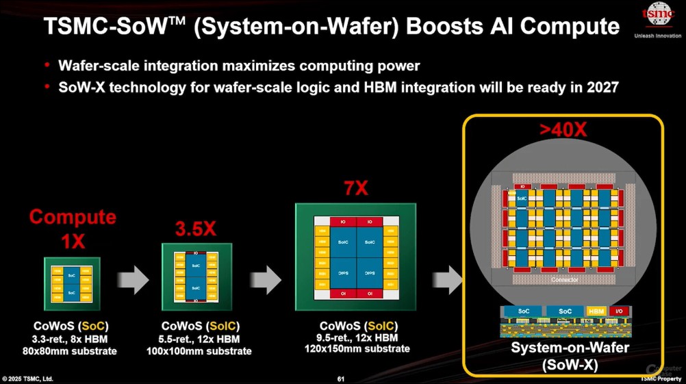
Tianfeng International analyst Ming-Chi Kuo posted an article on X (formerly Twitter) on the 11th, proposing five key analyzes on TSMC’s next-generation advanced packaging technology CoPoS (Chip-on-Panel-on-Substrate), and specifically clarified three common misunderstandings. CoPoS is a panel-level packaging technology being developed by TSMC. The current mainstream CoWoS (Chip-on-Wafer-on-Substrate) packaging is based on 12-inch round wafers and has limited available area. As the mask size of AI wafers continues to increase (for example, Rubin GPU has reached 5.5 times the mask size), a single wafer can only package 4 to 7 wafers, and the production capacity bottleneck is becoming increasingly severe.
The core concept of CoPoS is to convert the packaging carrier from a circular wafer to a rectangular panel. Taking a 310mm × 310mm panel as an example, the usable area is more than 5 times that of a 12-inch wafer. It can integrate more HBM stacks, I/O small chips and computing dies at the same time, greatly improving packaging density and output efficiency.
TSMC’s #CoPoS is moving fast, and the opportunities for Taiwan suppliers are taking shape. CoPoS replaces traditional round glass carrier with a square panel format, pushing utilization rates above 75%.
More on glass material development: https://t.co/Na9XtpNK8Q 🔗 pic.twitter.com/vam2gform8— TrendForce (@trendforce) June 12, 2026
CoWoS to CoPoS: paradigm shift from wafer to panel
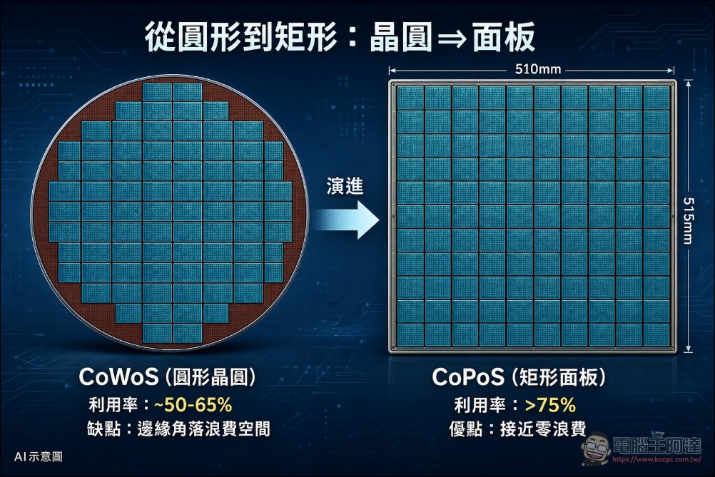
To understand the revolutionary nature of CoPoS, we must first understand the limitations of current CoWoS. TSMC’s CoWoS technology is the current mainstream solution for AI chip packaging, and Huida’s H100 and B200 series GPUs all use this technology. However, CoWoS is based on a 12-inch (300mm) circular wafer, and the effective utilization area is limited by the geometry of the wafer. Taking Huida’s next-generation Rubin GPU as an example, its mask size has reached 5.5 times, and only about 4 to 7 chips can be packaged on a 12-inch wafer. As AI models continue to expand, the requirements for the number of HBM stacks and die integration have only increased, and the capacity ceiling of circular wafers can no longer meet demand.
CoPoS solves the two major bottlenecks of area and efficiency at once by converting the packaging carrier from a circular wafer to a rectangular panel. The utilization rate of rectangular panels is much higher than that of circular wafers, and the panel size can be expanded according to demand (currently planned to be up to 510mm × 515mm), leaving ample room for upgrades to larger-sized AI chips in the future.
Analysis of Ming-Chi Kuo’s Five Key Points
1. Mass production schedule and target applications
Ming-Chi Kuo pointed out that CoPoS is currently expected to enter mass production in the second half of 2028, and is designed for ultra-large packages with a mask size of more than 9.5 times. Feynman, Huida’s next-generation AI chip, is expected to be the first adopter. According to the Business Times, TSMC’s CoPoS experimental line has been handed over to the R&D department in February 2026. The complete production line is expected to be completed in June, and the Chiayi AP7 factory has been selected as the mass production base.
2. Two uses and sizes of glass
According to industry surveys, glass materials in CoPoS are used in two different places:
- 310mm × 310mm temporary glass carrier(Temporary Glass Carrier): used for support and fixation during the manufacturing process
- 250mm × 250mm (trial production) / 510mm × 515mm (mass production) glass panel: After processing, it is cut into independent glass core substrates
3. Three-layer structure of glass core substrate
Ming-Chi Kuo emphasized that the glass core substrate is essentially a sandwich structure: there is a glass core in the middle, and the upper and lower sides are covered with an ABF (Ajinomoto Build-up Film, Ajinomoto insulating film) layer, which is the so-called ABF-GCP (Glass Core Package). Widely discussed glass processing challenges in the industry, including TGV (Through Glass Via) forming and copper filling/metallization, are related to this structure.
4. The leading advantage in mass production is expected to extend to 2032
Ming-Chi Kuo believes that CoPoS should be able to continue and strengthen TSMC’s leading position in the advanced packaging field, and the visibility of potential advantages will be extended to around 2032.
Three common misunderstandings clarified at once
Ming-Chi Kuo highlighted three common misunderstandings about CoPoS in the industry and clarified them one by one:
Misunderstanding 1: CoPoS uses glass interposer
In fact, glass does not act as an intermediary. The interconnection function is responsible for the RDL (Redistribution Layer) on the chip side, plus the TGV/copper interconnection and the ABF build-up layer in the glass core substrate.
Misunderstanding 2: Glass replaces ABF
This is wrong. It can be seen from the above three-layer structure that glass and ABF coexist, not replace each other. ABF still plays a key role in the layer-added process.
Misunderstanding 3: The chip is placed directly on the glass
The wafer is actually attached to the ABF buildup of the glass core substrate rather than directly touching the glass.
Warpage problem is the biggest challenge in mass production
The biggest technical problem faced by CoPoS is the warpage problem. The semiconductor industry pointed out that as the packaging substrate area increases, the difference in thermal expansion coefficients between various materials will cause stress imbalance, and the problem will worsen non-linearly as the packaging area and the number of RDL layers increase.
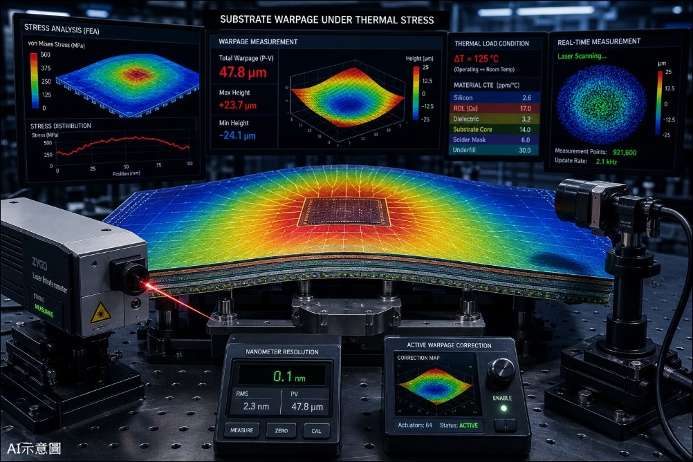
TSMC is using an alliance model to drive Taiwan’s supply chain to jointly overcome this problem. On the material side, Santaishi provides a Balance Film solution that offsets package deformation through reverse stress; on the equipment side, Printer Technology focuses on warpage correction and high-precision process control. According to legal analysis, the formation of this wave of localized supply chains will help reduce geopolitical risks, and is also regarded by the industry as the key to the formation of the “mountains that protect the country.”
NVIDIA Feynman: CoPoS’s first customer?
Ming-Chi Kuo specifically mentioned in his post that Feynman, Feynman’s next-generation AI chip, is expected to be the first adopter of CoPoS. According to TechPowerUp reports, Huida plans to use the larger panel area to integrate up to 12 HBM4 memory stacks in a single package, paired with multiple GPU computing dies, to bring significant performance improvements to AI workloads.
Meanwhile, AMD and Broadcom will continue to use TSMC’s CoWoS-L and CoWoS-R variants for their high-end products. This means that CoWoS will still be the mainstream in the short term, but the introduction of CoPoS will provide a new solution for ultra-large packaging needs.
Differences between CoPoS and CoWoP
The industry often confuses CoPoS with CoWoP (Chip-on-Wafer-on-Panel). The key difference between the two is the packaging carrier: CoWoP is still based on the wafer-level process, but replaces the substrate with a panel; while CoPoS completely shifts from the wafer-level process to the panel-level process (Panel Level Packaging), covering all packaging steps such as RDL and build-up layers. Panel-level packaging not only brings area expansion, but also reduces unit costs and improves output efficiency.
關於台積電的次世代先進封裝 CoPoS 的幾個關鍵(省略可查詢到的技術細節):
1. 預計 2H28 量產,目標提升 9.5 倍光罩尺寸以上的封裝之量產經濟性,Nvidia 的 AI 晶片 Feynman 可能將首度採用。
2. 根據產業調查,兩個不同的地方會用到玻璃(尺寸 mm):
→ 310 x 310 的臨時玻璃載具(glass…— 郭明錤|Ming-Chi Kuo (@mingchikuo) June 11, 2026
Industry timeline organization
- February 2026: The CoPoS experimental line begins to be handed over to the R&D department
- June 2026: The complete trial production line is expected to be completed
- 2027: The trial production line continues to optimize the process to meet the needs of partners
- Second half of 2028:Target mass production schedule, Chiayi AP7 factory
- 2029: The first batch of products equipped with CoPoS packaging are expected to be launched
- ~2032: CoPoS continues TSMC’s visibility scope in advanced packaging leadership
Against the background of the continuous explosion of AI computing demand, advanced packaging has been upgraded from a back-end process in the past to a core link that affects the overall industry competitiveness. Whether CoPoS can be implemented as scheduled will determine whether TSMC can maintain its absolute leadership in next-generation AI chip packaging.
Source: KOCPC Chinese