


At the Google Cloud NEXT ’26 conference held in Las Vegas, Google officially unveiled its eighth-generation TPU AI accelerator chip. Departing from the previous “one generation, one chip” convention, Google adopted a “dual-track” approach, unveiling in one go a solution designed for extreme training TPU 8t(code name Sunfish) and one specializing in massive inference TPU 8i(Code-named Zebrafish). Facing the industry’s shift from generative AI to a new phase of “AI Agents” and “agentic workflows,” these two chips will become the new core of Google Cloud’s “AI Hypercomputer.”
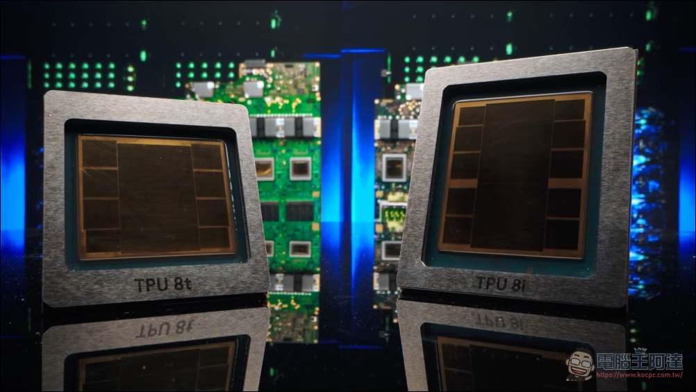
Google Cloud Next ’26 Unveils 8th Gen TPU: Inference and Training Running in Parallel
Google Cloud CEO Thomas Kurian pointed out at the conference that we are entering a new era of the “agentic enterprise.” In this era, AI is no longer just simple chatbots, but intelligent entities capable of complex reasoning, executing multi-step workflows, and self-learning in continuous loops.
Google CEO Sundar Pichai also shared some striking data: Google has internally implemented “agentic workflows,” and currently, up to 75% of all new code at Google is generated by AI and approved by engineers—a significant jump from 50% last fall.
Because AI agents need to handle very long context windows and complex logical reasoning, this presents distinctly different demands on the underlying hardware: training requires extreme compute throughput and horizontal scalability, while inference places greater emphasis on memory bandwidth and response latency. TPU 8’s dual-track design is precisely engineered to achieve the optimal balance between cost, performance, and power consumption.
TPU 8t: Accelerate Training Cycles, Build Performance Engines for Frontier Models
The core design of the TPU 8t (Training) is to reduce the development time of cutting-edge models, shortening tasks that originally took months to within weeks.
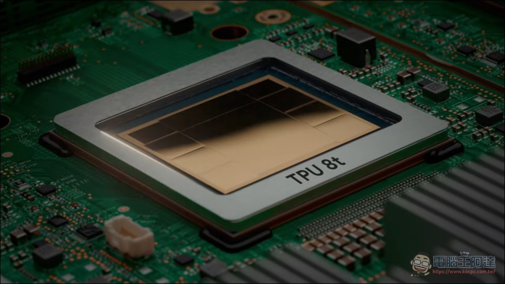
Remarkable compute density and 3D Torus topology
TPU 8t adopts Google’s proven 3D Torus network topology, but achieves a massive leap in scale. A single “Superpod” can now accommodate 9,600 chipsand provide up to 2 PB (2,000 TB) of shared High Bandwidth Memory (HBM)Under the latest FP4 precision, a single rack’s computational performance has reached 121 ExaFlops 。
2. Native FP4 and SparseCore Optimization
To break through memory bandwidth bottlenecks, the TPU 8t introduces native FP4 (4-bit floating point) operations, which doubles the throughput of the chip’s Matrix Multiply Unit (MXU). Additionally, the TPU 8t features a dedicated “SparseCore” accelerator specifically designed to handle irregular memory accesses common in Embedding lookups. This design effectively prevents the “zero-op bottlenecks” commonly seen when processing large-scale recommendation systems or language models. [3]。
3. Virgo Network: Near-Linear Scaling to a Million Chips
Google simultaneously announced a new data center network technology called “Virgo Network.” This is a network architecture with extremely high port density, and paired with the JAX and Pathways software frameworks, the TPU 8t is capable of supporting up to in a single logical cluster 1 million chipsGoogle claims that even at such a massive scale, Virgo can still provide near-linear performance scalability, solving the communication latency issues commonly seen in distributed training.
TPU 8i: Low-Latency Inference, the Instant Brain for AI Agents
The TPU 8i (inference type) is purpose-built for large-scale, high-sensitivity inference workloads, featuring deep optimization for today’s mainstream Mixture of Experts (MoE) models.
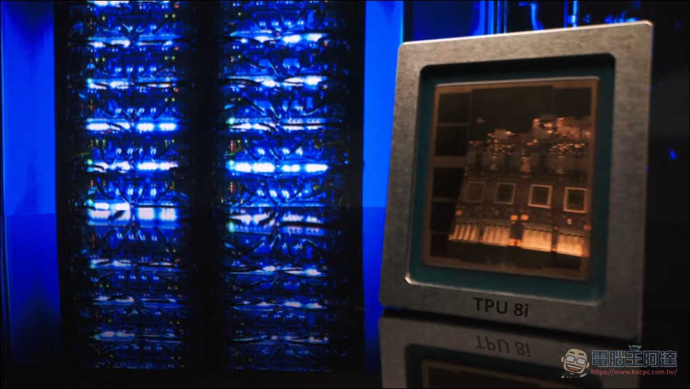
1. SRAM capacity tripled, data “stays on-chip”
Inference processes suffer from latency primarily due to frequent data movement. The TPU 8i is equipped with 288GB of HBM and Gundam 384 MB internal SRAMSRAM capacity is more than three times that of the previous generation inference chip (Ironwood), allowing the model’s working set to be fully stored on-chip during operation, significantly reducing dependence on external memory and enabling real-time responses.
2. Enhanced chip interconnect bandwidth
For the MoE architecture, TPU 8i increases the inter-chip interconnect bandwidth to 19.2 TB/sensuring that AI agents can execute multi-turn dialogue and reasoning tasks with extremely low latency when multiple chips work together. At the single Pod scale, TPU 8i can accommodate 1,152 chipsEach Pod’s FP8 computational performance is 11.6 ExaFlops 。
Technical Highlights: Axion CPU Integration and Fourth-Generation Liquid Cooling
To completely eliminate system-level bottlenecks, the TPU v8 series also introduced innovations on the host side:
- Drop x86 and adopt AxionGoogle has abandoned traditional x86 host processors this time, opting instead for its own Arm-based architecture. Axion CPUThis not only improves data preprocessing efficiency (reducing access latency by 10x), but also further optimizes the overall energy efficiency ratio of computing power.
- Energy efficiency doubledThrough fourth-generation liquid cooling technology and system-level co-design, TPU 8 maintains powerful compute performance while delivering improved performance per watt compared to the previous generation. 2 timesThis is crucial for maintaining net-zero carbon emission goals while competing in the AI compute race.
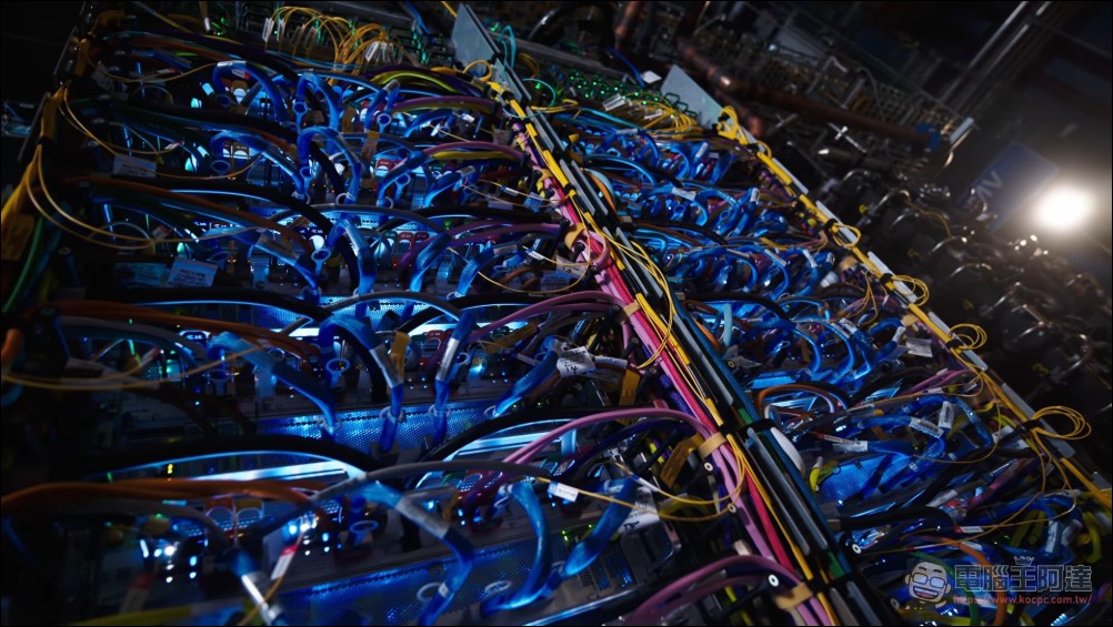
MediaTek ASIC Orders Bring Good News for Taiwan Supply Chain
As Google expands its TPU deployment, Taiwan’s supply chain is also benefiting significantly. Market expectations are thatMediaTek (2454) Successfully secured ASIC foundry orders for inference chips (TPU 8i series), and responsible for the corresponding physical design and silicon IP integration.
Boosted by this news, MediaTek’s stock price showed strong momentum on the 22nd, closing at the daily limit-up price. NT$2,295 Closing at a record all-time high. Besides MediaTek, thermal, substrate, and optical communication suppliers including Unimicron, Gold Circuit Electronics, Powertech, and Innolux have also gained significant market attention for being part of Google’s AI supply chain.
NVIDIA Face-Off: Compute Power vs. Scale
Although NVIDIA’s upcoming Rubin GPU still outperforms a single TPU v8t in FP4 training performance (approximately 35 PetaFLOPS) when looking at chip-level performance alone, Google is emphasizing “system-level” advantages.
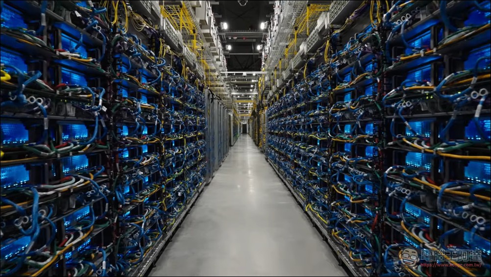
NVIDIA’s NVLink domain is limited to 576 GPUs within a single supercomputing node, requiring Ethernet-based expansion beyond that; Google’s TPU 8t, leveraging optical switching technology, can directly connect 9,600 chips in a single unified domain, scaling even to the millions. For developing massive frontier models like Gemini, this “large pool memory” architecture offers natural advantages in communication latency.
Scheduled for official release in the second half of 2026
Google announces that TPU 8t and TPU 8i are expected to late 2026 Officially launching on Google Cloud for enterprise use. At that time, enterprise customers will be able to choose the most suitable “AI tools” based on their own needs. Whether it’s R&D teams that need to burn the midnight oil training new models, or operations teams that need real-time responses managing countless AI agents, all will have the most powerful computing support.
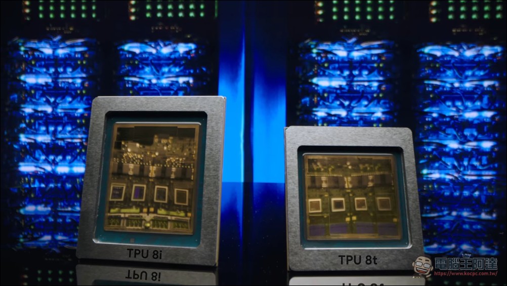
As computing costs continue to optimize, we are witnessing AI’s evolution from a “consulting tool” to an “execution agent” at a critical turning point, and Google’s eighth-generation TPU is precisely the core engine driving this revolution.
Source: KOCPC Chinese