


This site has previously reported on the CMP 170HX card.News that it was cracked by software aloneAt the time, the research team exploited the vulnerability to break the topmost signature verification in a three-layer trust stack. After gaining HS mode permissions, they rewrote the privilege-level mask. After the modification, FP32 rose from 0.39 TFLOPS to 94 TFLOPS—about a 31× improvement—and memory expanded from 10GB to 80GB, which also caused the price of the 170 HX to soar severalfold within just a few days. But three clear ceilings remained at the time: PCIe Gen3 could never be enabled; the AC coupling capacitors for the 12 lanes omitted on the PCB had to be manually supplemented by soldering 24 100nF capacitors to restore the x16 physical connection; and HBM mode registers and on-die ECC were likewise locked by Source ID. The paper’s authors were careful at the time, saying the status of these limitations was “no method found” rather than “proven unbreakable.” Recently, American hardware researcher Kate publicly disclosed on her personal blog a voltage fault injection vulnerability in the GA100 chip. She used this vulnerability to blow the fuses NVIDIA uses to lock features, turning a CMP 170HX mining card that originally had only 8GB into an accelerator card with 80GB of memory and more than 120 SM compute units. FP16 performance reached 85.9 TFLOPS, and its AI performance even beat a retail A100 priced at $20,000.
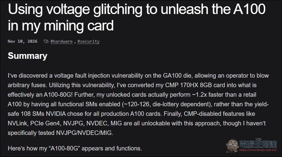
The open-source code, STM32 firmware, and hardware design files for this method have also been made public on GitHub, and the schematic for the control board responsible for generating voltage pulses was designed with the help of GPT-6 Astra.
GA100VFI:GA100 voltage glitch resources – GitHub
From software unlocking to hardware attacks
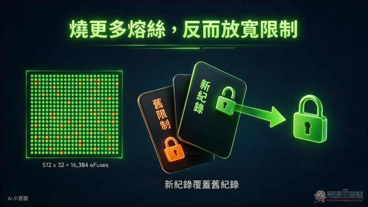
Kate’s approach cuts directly into the hardware layer and pushes past all three ceilings at once. She discovered a structural issue in NVIDIA’s fuse design on the GA100: the GA100’s fuse controller contains 16,384 eFuses, forming a 512-row by 32 array. Among them is a special “fuse-less fuse” block that uses a record format similar to a JTAG chain; at boot, the controller replays it in sequence to determine the value of the final option string.
The key here is that records are written with overwrite semantics. As long as a new record is written pointing to the same location, the old restriction will be cleared, and the physical fuse does not need to be “blown back to unblown.” In a normal design, burning a fuse can only tighten permissions, but on GA100, burning more instead loosens restrictions. Kate sums up in one sentence how insecure NVIDIA’s design is: burning a fuse can give you more functionality, not less.
To burn these fuses, you first have to disengage a gate. The controller has a OPT_SECURED_BURN_FEATURE_ENABLE Option strings: all production cards are enabled; when enabled, only a specific range of fuses can be written, and the no-fuse fuse area is completely locked down. Using voltage fault injection, Kate triggered a glitch state she calls Goldilock, causing all option strings derived from the control row to read as zero, and then used SENSE_CTRL The command causes them to return to the original fuse values, but retain DISABLE_SW_OVERRIDE to zero, so that a software override can shut that gate off.
That board that GPT-6 Astra helped design.
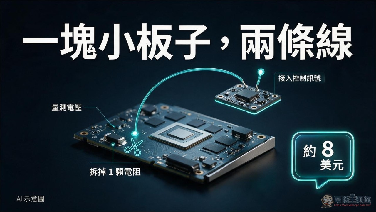
The execution tool for the entire attack was a custom-designed STM32G431 control board. Kate explains in the article that she asked GPT-6 Astra to design an STM32G4 board capable of interfacing with PWMVID signals. PWMVID is NVIDIA’s standard communication protocol for voltage regulators. This board intercepts the PWM signals sent by the GA100 chip and instead feeds its own waveform to the MP2888B voltage regulator driver IC, causing the graphics card’s own VRM to generate precisely timed voltage pulses.
The installation method is quite primitive. The entire device makes only two connections to the PCB: one measures the NVVDD voltage, and one taps into the PWMVID signal; ideally, these are magnet wire held in place with magnets. The only place that requires a soldering iron is removing a 0402-size 0-ohm resistor, cutting the connection between the GA100’s PWM output pin and the voltage regulator. The chip itself costs about $8.
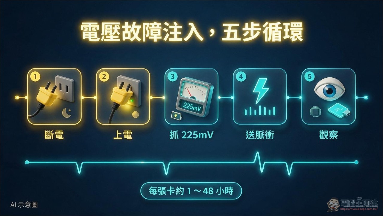
Each attempt proceeds like this: power off, power back on, use a comparator to detect the moment NVVDD crosses 225mV and start a timer, send the designed voltage waveform according to the timing, and observe the graphics card’s response. She uses ACPI power-state transitions from S0 to S3 and back to S0 to power off and restart, allowing a cycle every few seconds. A card usually takes one to 48 hours of glitching to succeed.
The numbers that outperform the A100, and its limits.
The comparison table Kate included in the article is the part most worth reading this time:
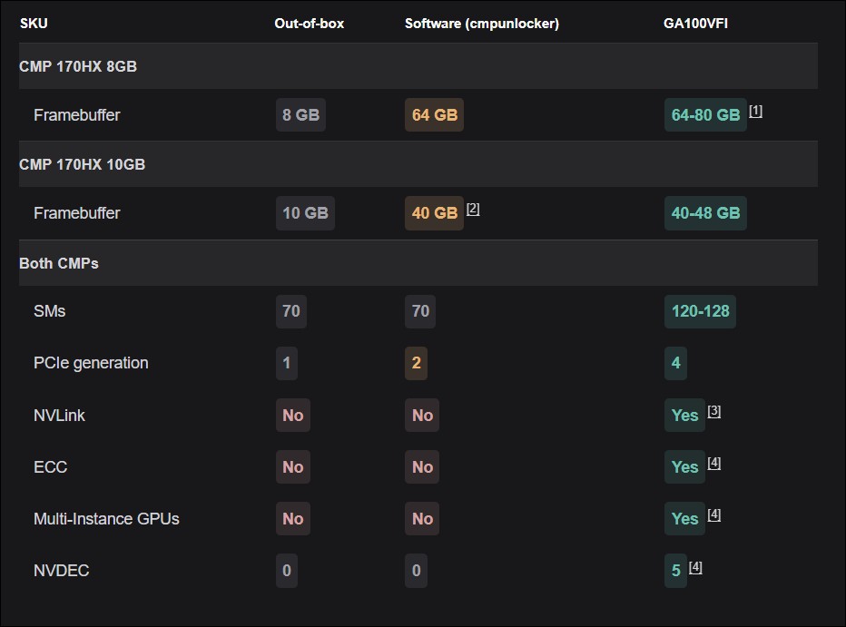
- Memory of the 8GB versionFactory 8GB, software-unlocked to 64GB, 64 to 80GB after voltage attack
- 10GB memory version10GB from the factory, software-unlocked to 40GB, and 40 to 48GB after a voltage attack.
- SM compute unitFactory: 70, software unlock: 70, after voltage attack: 120 to 128
- PCIe generationFactory Gen1, software-unlocked Gen2, Gen4 after voltage attack
- NVLink, ECC, Multi-Instance GPUNeither of the first two; it turns on after a voltage attack.
The performance numbers come from ProjectPhysX’s OpenCL benchmark: after the software unlock it is 50.1 TFLOPS FP16, retail A100 is 72.5, and the mining card after the voltage attack is 85.9, about 1.18 times an A100 and 1.7 times the software-unlocked version. Kate says real inference frameworks such as vLLM and SGLang can run on the full 80GB.
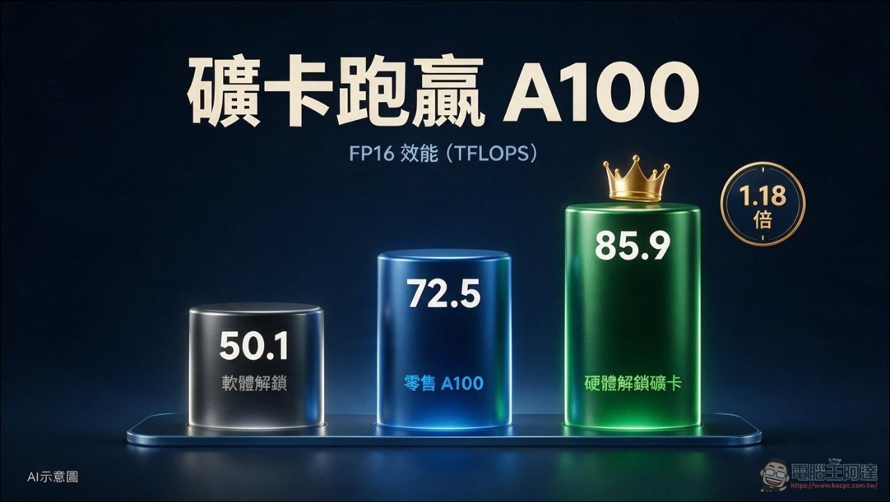
The reason its compute performance can surpass the A100 lies in wafer yield. The GA100 ships with 128 SMs, but to ensure yield, NVIDIA enables only 108 on all mass-produced A100s. Most of these SMs judged defective are actually good on the chip and are simply disabled by fuses. Kate’s unlock brings them back online, with the number ranging from 120 to 126 depending on the wafer batch.
The three restrictions must be clearly stated.
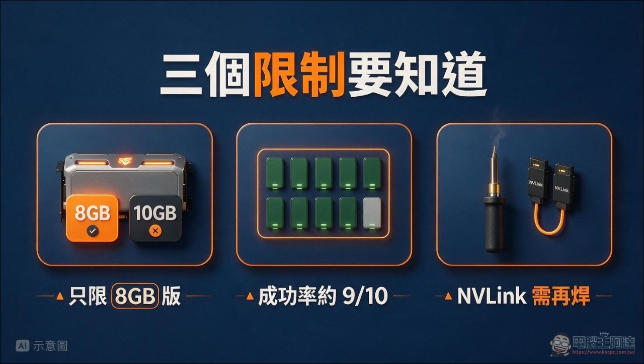
First, 80GB only applies to the 8GB version. Kate notes in a footnote that the 10GB version is packaged with 4 HBM stacks, while the 8GB version has 6; these are two different physical configurations. The community-maintained CMP 170HX technical wiki also clearly states that after unlocking, the 8GB card is 64GB and stable, while the 10GB card after unlocking is 40GB and stable, and the two cannot replace each other. The same wiki records that the community once tried to push the 10GB card to 81920 MiB, but folding occurs at 40 GiB; memory validation beyond 39GB has never been reproducible and triggers an Xid error that makes the GPU vanish on the spot. Kate’s own footnote also says that the paper “Canary in the Crypto Mine” claims the 10GB version can stably run 80GB, but almost no cards have achieved this, and the evidence is scarce.
Second, the success rate is not 100 percent. Of the 10 8GB cards Kate checked, 9 had the full 80GB of memory, while the remaining 1 had only 64GB usable from the factory, and even after that card was successfully unlocked, its memory capacity did not increase at all.
Third, NVLink will require another round of soldering. Clearing the NVLink disable string is only the first step. The CMP 170HX PCB lacks U11, the IC that connects PCIe 3.3V to the NVLink bridge pins, so production boards cannot start the bridge’s reference clock generator; this can only be solved by shorting the two pins at that location with a jumper. Kate warns that this will tie together the 3.3V power rails of cards on different power supplies unless one of the cards is left with U11 unsoldered. Achieving PCIe Gen4 x16 likewise requires a decoupling capacitor modification.
Must-Know Price Spreads and Risks
In the Taiwan market, retail pricing for the A100 80GB PCIe is quite transparent. AUTOBUY’s shopping center lists a custom-order item at NT$735,000, while on Shopee and Yahoo Auctions, quotes for Taiwan company goods range from NT$462,000 to NT$652,000. Taiwan distributor EDOM Technology lists the A100 80GB PCIe specifications as 80GB HBM2e, 1,935 GB/s memory bandwidth, and 300W maximum power consumption; it uses a passive cooling design and requires chassis fans for assistance.
By contrast, the secondhand price of the 8GB CMP 170HX has already surged in both Taiwan and the global market. At the time of Tom’s Hardware’s report, the 8GB version was around $3,000 and the 10GB version around $2,500, which is already 60% of the $5,000 per-card price when that card launched in 2021. The price curve tracked by the community on X was about $200 last year, $1,500 last month, and over $3,000 this month. The figures recorded in our August article at the time were a transaction price of about RMB 3,000 to 4,000 in China’s secondhand market and an eBay listing of about $1,500.
All told, a $3,000 mining card plus a self-soldered modification comes to roughly one-sixth to one-tenth of the hardware cost of a retail A100 80GB. The trade-off is that each card has to be powered on for one to two days, may be permanently burned out, and you have to take on the risk of soldering and modifying the BIOS yourself.
Conclusion
The significance of this release lies in reproducibility. Kate has provided a 29KB technical document plus the complete open-source code, including KiCad schematics, STM32G431 application firmware, a custom USB bootloader, the PWMVID host control tool, the GA100 register capture engine, and the glitch experiment workflow. Anyone capable of soldering can follow it; the only barriers are time and soldering skill.
This also means that a hard-to-fill gap has appeared in NVIDIA’s product segmentation strategy. The GA100 chip has 128 SMs but only 108 are enabled; the 8GB mining card packages 80GB of memory but only exposes 8GB. These were decisions made at the time for cost control and yield management. When the locking mechanism can be cracked with a device costing a few hundred dollars, every chip shipped in a downgraded configuration on the market becomes a hidden high-end product.
For AI compute users in Taiwan, the most practical information right now is price. A retail A100 80GB costs NT$460,000 to NT$730,000, and the memory market remains tight because of AI demand. Under this supply-demand structure, people who can solder have an extra gray-market channel for getting large memory. Those who know how to use them have long known these mining cards exist. What happens next is prices continuing to rise, and more people who lack the patience to solder buying secondhand mining cards outright, only to find they can’t handle it and waste money. We personally don’t recommend anyone take the risk and try.
Source: KOCPC Chinese