


SemiAnalysis, a well-known foreign semiconductor independent research institution, recently published the latest public report of its disassembly laboratory STEEL (SemiAnalysis Teardown Engineering and Evaluation Lab), which conducted a reverse engineering analysis at the electron microscope level for Huawei’s latest flagship Kirin 9030 chip released last year. It was found that without EUV (extreme ultraviolet lithography) equipment, SMIC’s third-generation 7-nanometer process N+3 achieved a minimum metal pitch of 32.5 nanometers, which is about 10% thinner than the 36 nanometers used in Intel’s latest 18A process on Panther Lake.
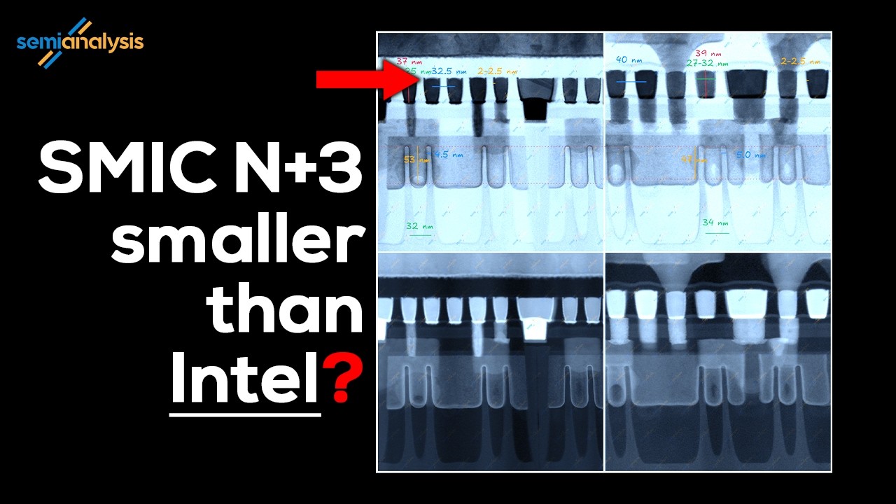
Huawei Kirin 9030 dismantling: SMIC SMIC 7nm metal line width is already thinner than Intel 18A
This report also echoes some of the details mentioned in the Kirin 9030 Pro published by Geek Bay a while ago, but this report also points out that,Thinner linewidths do not equal better chips. The N+3 has indeed caught up with the TSMC N6 in terms of pure density, but there is still a clear gap in power consumption and performance. SemiAnalysis concluded: Export controls do not stop China, but change the problems China is solving.
Who is STEEL Labs?
STEEL is a wafer disassembly laboratory built by SemiAnalysis in Oregon, USA. It took a year and a half to build. Dylan Patel, CEO of SemiAnalysis, pointed out that for the past 20 years or so, large-scale chip reverse engineering has basically been done by one company (TechInsights). TechInsights, currently owned by private equity, is being sold and a chronic lack of competition has led to underinvestment in capital expenditures. With no outside investors and just six years old, SemiAnalysis has surpassed TechInsights in revenue.
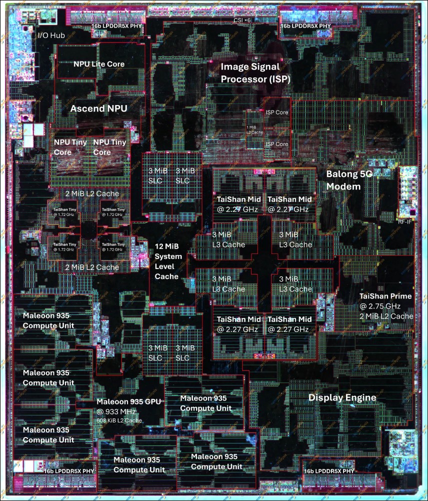
STEEL this timeTeardown reportAll data, including cross-sections, linewidth measurements, and transistor counts, come from laboratory electron microscopy analysis. This is also STEEL’s first public report, and more disassembly results will be released in the future.
32.5 nm vs. 36 nm: The truth behind the numbers
Kirin 9030 uses SMIC’s N+3 process, which is China’s most advanced semiconductor process. SemiAnalysis also disassembled MediaTek Helio G99 (based on TSMC N6 process) as a control group, because TSMC N6 and SMIC N+3 belong to the same generation of nodes, one is manufactured using the most advanced equipment in the West, and the other is produced locally in China under export controls. Measurement results show that the minimum metal pitch of Kirin 9030 is 32.5 nanometers, and that of TSMC N6’s Helio G99 is 40 nanometers. The gap is quite significant. In terms of pure density, N+3 reaches about 113 million transistors per square millimeter and TSMC N6 about 108 million. That said, a SMIC’s DUV nodes are indeed denser than an EUV node.
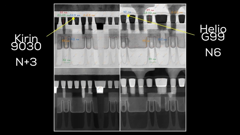
But SemiAnalysis emphasizes that the thinner line width is a statement about density, about how many logic circuits can be crammed into each square millimeter, rather than a judgment about the overall quality of the chip or process node. Minimum metal spacing is only part of the equation; it does not represent logic switching speed or power consumption performance.
How to do it without EUV? Both techniques have their own costs
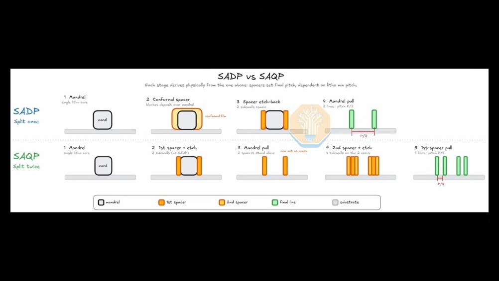
To achieve EUV-level density without EUV, SMIC uses two core tricks. The first is multi-patterning. EUV can print a fine pattern in a single exposure, but DUV must be done in steps: printing a rough pattern first, depositing a thin spacer layer along the edges, and then etching using the spacer layer itself as a new, finer mask. Doing it once is called self-aligned double patterning (SADP), and doing it twice is called quadruple patterning (SAQP). SMIC’s densest metal layers require quadruple patterning, and each additional step creates an additional layer of masking, an opportunity for alignment error, higher cost, and lower yield.
The second technique is DTCO (Design Technology Co-Optimization), which is to optimize chip design and manufacturing technology together instead of treating them as independent problems. Practical practices include reducing the number of fins per transistor, placing the gate contacts directly above the active gate instead of offset, and reducing the isolation gap between adjacent cells. Each DTCO trick reclaims a little area, but also makes the transistor more fragile and harder to model.
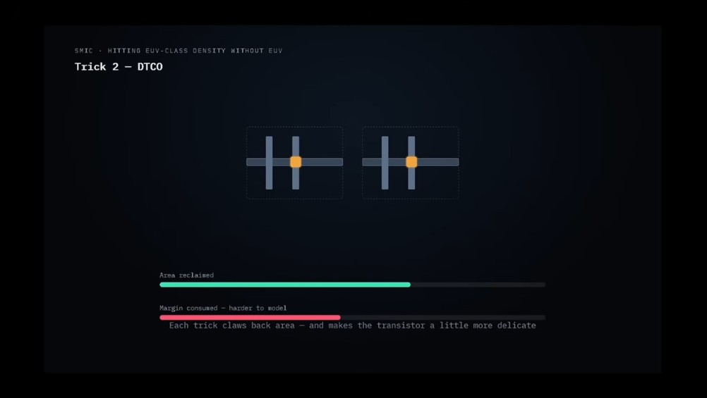
Density wins, efficiency loses
Density improvement is an “easy” axial improvement. Since the demise of Dennard’s scaling law in the mid-2000s, simply shrinking transistors has failed to deliver both speed and efficiency gains. Under the DTCO framework, speed and efficiency must be fought for separately, and both cannot be given consideration at the same time. This is the reality of the N+3 process: the performance of the Kirin 9030 Pro is roughly equivalent to that of Android flagships from three years ago.
The most striking contrast comes from Apple’s efficiency core. Apple’s small E-core beats Huawei’s large-core Prime core in integer performance, but consumes only about 1 watt compared to 4.5 watts. The performance per clock of the Huawei Prime core falls approximately at the level of the Arm Cortex-X2, which is a 2021 design. Apple’s 2020 M1 is still about 35% faster per clock at similar power consumption. The current leading flagship is far ahead.
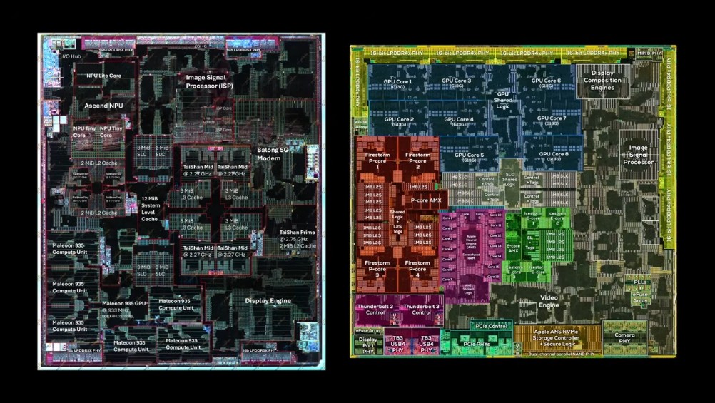
The comparison with the Intel 18A is equally intriguing. 18A is on paper capable of 32nm M0 metal pitch, on par with N+3. But on Panther Lake, Intel is heavily adopting looser high-performance cell configurations at 36nm because looser metal spacing reduces costs and improves yields. Having the freedom to choose where and how to scale is an advantage in itself. The backside power delivery technology of Intel 18A allows the introduction of power connections on the back of the chip, further freeing up the metal layout space on the front. This is a capability that N+3 currently does not have.
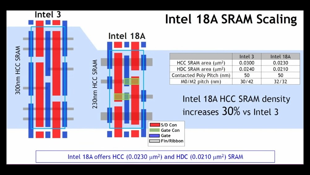
The road ahead: The wall gets steeper and steeper
SemiAnalysis noted that SMIC still has room to grow in the DUV route. The future N+4 can roughly match the density of TSMC N5 level, and N+5 plus the power supply technology behind it can reach the density of Intel 18A level. But the difficulty of each optimization is cumulative, and each new node is slower, more expensive, and less error-prone than the previous one. “You can keep climbing the wall, but the wall will only get steeper.”
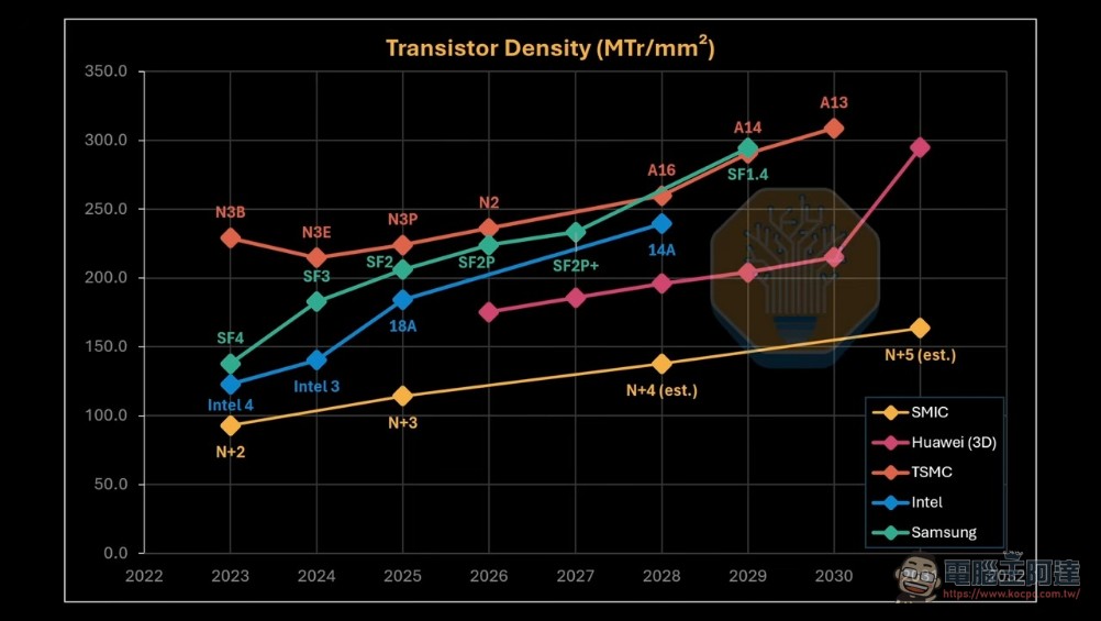
Knowledge diffusion is another issue that needs to be faced. SMIC is being directed to license the N+2 and N+3 processes to other local Chinese fabs. If process knowledge flows into the field of AI accelerators, the bottleneck will no longer be a single fab that can be sanctioned, but will become the entire ecosystem.
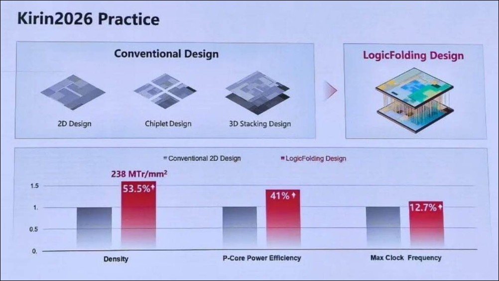
Huawei’s other path is through advanced packaging and system technology collaborative optimization (STCO), using technologies such as τ scaling and Logic Folding (which is what Huawei said beforeTao’s Law”), stacking active logic circuits at the package level and restoring density. This means that China’s semiconductor strategy is simultaneously finding a way out through two routes: process shrinkage and system architecture level.
There is also an official detailed video of the entire report. You can watch it with cc subtitles:
Conclusion
The teardown results of the Kirin 9030 reveal a complicated reality. On the pure density axis, SMIC does achieve thinner line widths than Intel, which is a real engineering achievement without EUV. However, “density” does not equal “energy efficiency” competitiveness. The gap between power consumption and performance clearly illustrates the huge gap between “doing it” and “doing it well”.
The final question raised by SemiAnalysis is worth pondering: China does not need to be TSMC to have an impact, it only needs to be “so good that it no longer needs TSMC”. When domestic chips are useful enough for mobile phones, reasoning, Internet and other applications, the meaning of export controls will be redefined. The final outcome of this semiconductor competition depends on whose ecosystem is more complete.
Source: KOCPC Chinese