


Samsung Electronics’ gallium nitride (GaN) semiconductor foundry business has hit another setback. According toForeign wire reportSamsung’s 8-inch GaN foundry line at its Giheung campus in Yongin, South Korea, has hit a snag — chips from the trial production phase cannot operate normally in high-temperature environments, and the original target of starting mass production by the end of the year may be pushed back by several more months. This is the second setback for Samsung’s GaN business in six months; back in May, its own GaN discrete components failed to secure orders because performance did not meet customer standards.
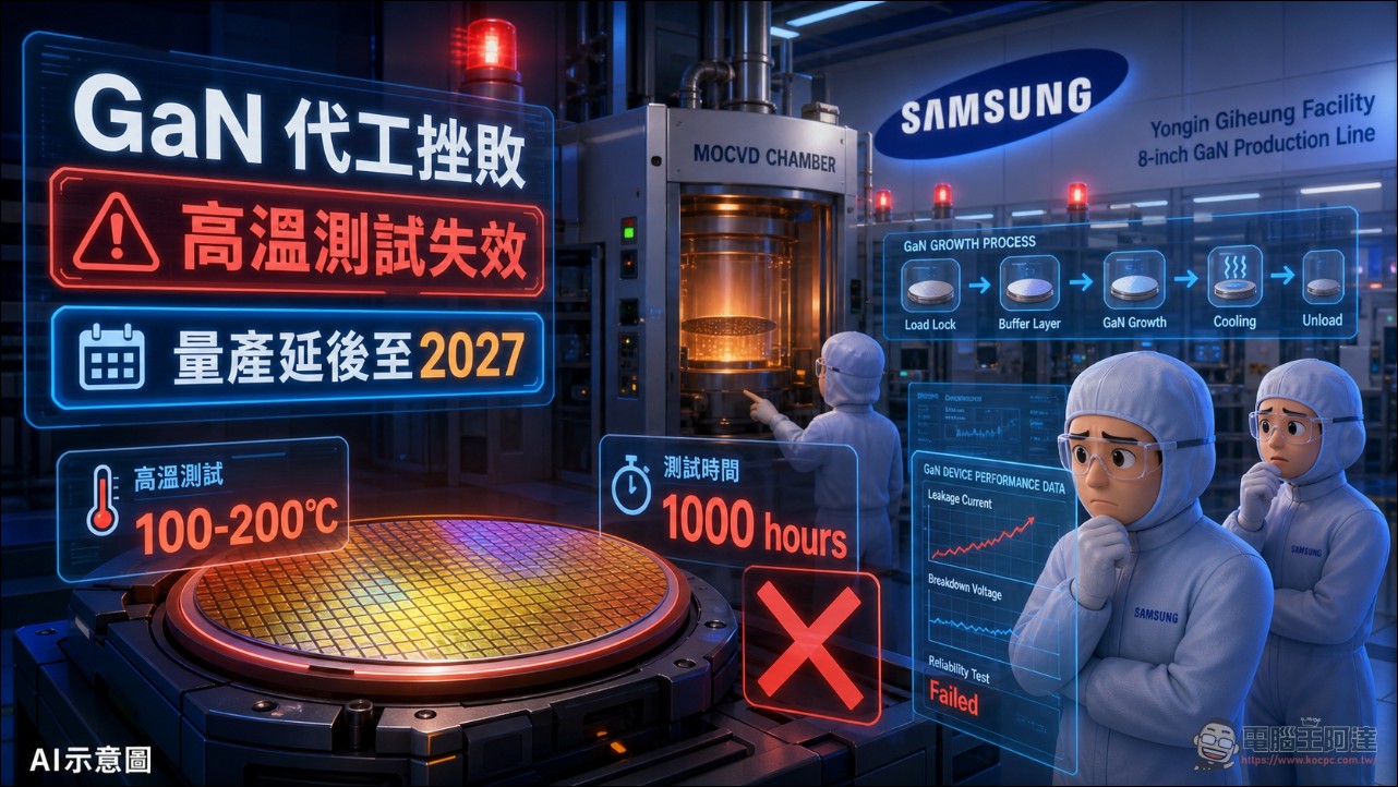
GaN is a next-generation compound semiconductor known for its high voltage tolerance, high-temperature resistance, and high switching efficiency. It is mainly used in applications that require high-voltage and high-temperature environments, such as electric vehicles, robotics, and data centers. Electric vehicle chargers and AI server power supplies may also use it. According to a report by Korean semiconductor media outlet The Elec, Samsung’s 8-inch GaN foundry dedicated line has a monthly capacity of approximately 1,300 to 1,500 wafers, producing chips for fabless chip design companies. However, after trial-produced chips were exposed to temperatures of 100 to 200 degrees Celsius for about 1,000 hours, they exhibited a phenomenon where they stopped operating.
Failed after just 1,000 hours of high-temperature testing.
GaN power components are designed for reliable long-term operation in high-temperature, high-voltage environments, supporting voltages up to 1,200 volts and ambient temperatures above 200°C. The test that failed this time is the HTOL (High-Temperature Operating Life) verification commonly used in the semiconductor industry: components run continuously for 1,000 hours under elevated temperature and voltage to confirm whether they drift out of specification or fail. This is a mandatory gate before shipment for applications such as onboard chargers, data center power conversion, and industrial motor drives. The trial-production chips could not survive 1,000 hours at 100–200°C, directly undercutting the core selling point of the GaN product line.
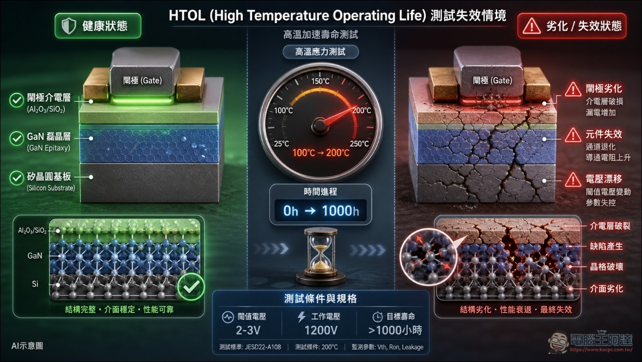
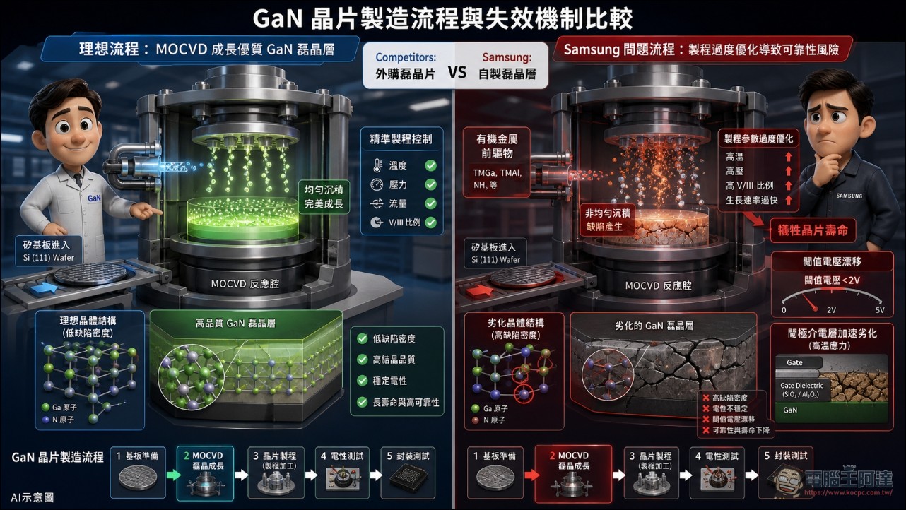
GaN wafers are produced by growing a gallium nitride epitaxial layer on silicon wafers using MOCVD (metal-organic chemical vapor deposition) equipment, and the quality of the epitaxial layer almost determines the performance and lifespan of the finished device. Industry insiders told The Elec that Samsung adjusted its process parameters to chase target performance, potentially at the expense of chip lifespan. GaN power semiconductors require a threshold voltage of 2 to 3 volts; if the voltage is set too low, the device may malfunction under tiny currents, and the gate dielectric layer will degrade faster under prolonged thermal stress, eventually causing device failure. Samsung produces its epitaxial layers in-house at Giheung, which gives it control over the supply chain and costs, but it cannot benchmark process recipes against third-party suppliers the way competitors can, so epitaxial process maturity must be accumulated from scratch.
Mass production schedule delayed twice, earliest mid-2027.
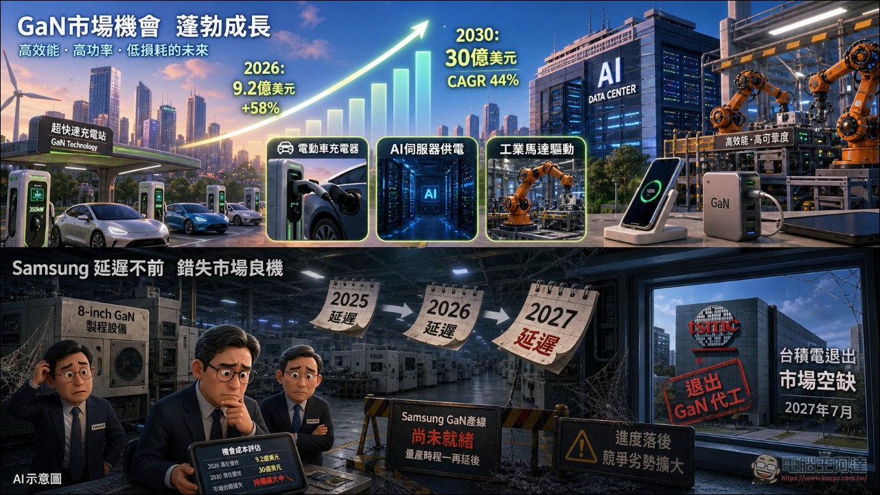
Samsung’s path in GaN has not been smooth. In 2023, Samsung reorganized its LED business, establishing a Compound Semiconductor Solutions (CSS) department focused on GaN. The GaN foundry line was originally scheduled to launch in 2025, but was postponed to the end of 2026 due to weak demand in the power semiconductor market. In May of this year, Samsung’s own 650V GaN discrete devices failed to meet customer performance standards for on-resistance, and after evaluation, multiple customers did not place orders. Samsung also simultaneously withdrew from the government-subsidized electric vehicle project with Semipowerex and abandoned its module business.
Following the HTOL test issue, the industry believes the mass production timeline could be delayed by several more months. The Tech Times analysis indicates that Samsung’s GaN foundry may not enter commercial mass production until mid-2027 at the earliest. Samsung officially responded that it is still in the pre-production development phase, working through trial-and-error issues before mass production, and that it is too early to determine whether this constitutes defective products.
Competitors have been shipping for one to two years, Samsung is clearly behind.
While Samsung was still figuring things out in the trial production stage, Infineon, STMicroelectronics, Texas Instruments, and China’s Innoscience had already been commercially selling GaN chips for one to two years. Infineon further announced in July 2025 that its 300mm (12-inch) wafer GaN process was progressing smoothly, with customer samples delivered in the fourth quarter of 2025. The 12-inch process yields 2.3 times more chips per wafer than the 8-inch process, and this cost advantage will directly pressure all 8-inch GaN programs, including Samsung’s. Innoscience is currently the world’s largest GaN-on-Si specialty manufacturer by production capacity.

Samsung’s potential customers are also taking a wait-and-see approach. The report notes that multiple fabless companies have already been evaluating other GaN foundry partners as backups, including GlobalFoundries, PSMC, and X-FAB. Mask costs for GaN semiconductors are far lower than for silicon wafers—a full mask set for an advanced silicon logic process can easily run into tens of millions of dollars, making it very difficult for customers to switch foundries once they’ve committed to tape-out. GaN mask costs are only a fraction of that, so having multiple foundries qualified simultaneously is a practical supply chain strategy. If Samsung fails to resolve its issues in a timely manner, its customer relationships could be gradually eroded by competitors.
In Korea, Samsung also faces pursuers. DB HiTek’s GaN foundry development plan continues to advance; in early 2026 it delivered evaluation samples to customers, targeting mass production in 2027. SK’s keyFoundry is also investing in the GaN foundry field. In other words, if Samsung’s GaN foundry keeps being delayed, not only may international customers switch to the GlobalFoundries and PSMC camp, but even the domestic Korean market could be preempted by DB HiTek.
The market is taking off, but Samsung can’t keep up.
The GaN power device market is in a period of rapid growth. According to market forecasts cited by Infineon, the GaN power device market is expected to reach $920 million by 2026, with an annual growth rate of approximately 58%. Driven by demand from AI data centers, electric vehicles, and fast-charging devices, the market is projected to approach $3 billion by 2030, with a compound annual growth rate of 44% from 2026 to 2030. In addition, TSMC announced in mid-2025 that it would exit the GaN wafer foundry business in July 2027, and the resulting market gap was initially seen as an opportunity for Samsung to step in. However, given Samsung’s current progress, it may be difficult for the company to fill that gap in time.
Conclusion
Samsung, leveraging its scale advantages in memory and wafer foundry, holds significant weight in the global semiconductor market, but on the new track of GaN, it has fallen far behind competitors due to a series of missed schedules, subpar performance, and reliability issues. Industry analysts point out that MOCVD process optimization is a highly experience-intensive engineering effort, with each round of testing, analysis, and parameter adjustments taking weeks. For Samsung’s GaN foundry to catch up, it faces a test of time and patience, and the window for market growth is shrinking quarter by quarter.
Source: KOCPC Chinese