


AMD dropped a shock bomb today (5/21), announcing that it will invest more than 100 million yuan in Taiwan’s industrial system. US$10 billion (approximately NT$320 billion), to expand strategic partnerships and increase advanced packaging manufacturing capabilities required for next-generation AI infrastructure. Following TSMC’s $165 billion investment in the United States, this is another time that Taiwan’s semiconductor industry chain has received an astronomical level of investment from a major international manufacturer. It also once again highlights Taiwan’s irreplaceable strategic position in the advanced packaging and AI supply chain.
The largest single foreign packaging investment in history: the strategic significance of US$10 billion
This investment of more than US$10 billion is AMD’s largest ever packaging and industry chain investment in a single country/region. Although AMD has not announced detailed allocations, the industry generally expects that funds will mainly flow to the construction of advanced packaging production capacity, including cooperation with Taiwanese packaging and testing manufacturers such as ASE, SPIL, and PTI to expand production, as well as production capacity support from carrier board suppliers such as Xinxing Electronics, Nanya Circuit Board, and Jingshuo Technology.
From an industry perspective, this investment comes at the height of the global AI arms race. Nvidia’s Blackwell/Rubin architecture GPUs also face a shortage of advanced packaging production capacity (CoWoS-L/CoWoS-R). AMD’s massive investment in Taiwan’s packaging ecosystem is equivalent to ensuring the mass production capabilities of the next generation of AI chips from the upstream. Compared with Nvidia, which relies heavily on TSMC’s CoWoS single packaging solution, AMD uses EFB technology to establish a second or even third packaging supply source in many packaging and testing factories such as ASE, Silicon Products, and PowerCenter. The supply chain resilience is obviously more advantageous. “By combining AMD’s leadership in high-performance computing with the Taiwanese industry and our global strategic partners, we are realizing an integrated rack-scale AI infrastructure,” AMD Chairman and CEO Dr. Lisa Su said in a statement.
EFB bridging technology: AMD’s packaging trump card against CoWoS
The core technology highlight of this investment is what AMD calls EFB (Embedded Fan-Out Bridge, embedded fan-out bridge) 2.5D advanced packaging technology. Different from the CoWoS (Chip on Wafer on Substrate) technology route led by TSMC, EFB is based on wafer-level bridge interconnection technology, embedding high-density interconnection layers into fan-out packaging substrates to achieve high-bandwidth, low-latency connections between small chips (Chiplets).
AMD revealed two major developments in a press release:
Cooperation with ASE: AMD is working with partners such as ASE and Silicon Precision to jointly develop and verify the next generation of wafer-based 2.5D EFB interconnect technology, which can significantly increase interconnect bandwidth and improve power consumption efficiency, providing strong support for the sixth-generation EPYC processor code-named “Venice”.
Breakthrough with LiCheng Technology: AMD and LiCheng Technology reached a major milestone and successfully verifiedIndustry’s first 2.5D panel-level EFB interconnect technology. Compared with traditional wafer-level packaging, Panel-Level Packaging can simultaneously package more chips on a larger area, greatly improving production efficiency and cost-effectiveness, allowing customers to deploy more efficient AI systems.
Compared with Nvidia’s current main CoWoS packaging technology (which has developed to the fifth generation of CoWoS-L), AMD’s EFB solution has a structural advantage in the diversity of packaging sources: CoWoS relies almost entirely on a single supplier, TSMC, while EFB can be mass-produced in multiple packaging and testing factories such as ASE, Silicon Products, and PowerCenter. This is a very critical competitive bargaining chip in the current market environment where advanced packaging production capacity is tight.
Venice EPYC and MI450X: performance beasts using N2 process
This investment has two heavyweight products as technology carriers. First of all, the code name “Venice“of6th Generation AMD EPYC Processors, based on the Zen 6 architecture and manufactured using TSMC’s N2 (2nm-level) process. This is also the first time AMD has pushed server CPUs to the 2nm generation. According to reports from TechPowerUp and Tweaktown, Venice’s CCD (core composite chip) uses TSMC N2P, and its IOD (input-output chip) uses N3P, forming a split-node strategy.
The second one is AMD Instinct MI450X GPU, based on CDNA 5 architecture and also using TSMC N2 process. The MI450 series is the industry’s first AI accelerator to break the 400GB memory barrier, equipped with 432GB of HBM4 memory, directly benchmarking Nvidia’s next-generation Rubin architecture. This is AMD’s first AI GPU using the N2 process, which has significant competitive advantages in energy efficiency.
Helios rack platform: multi-gigawatt deployment to begin in the second half of 2026
Powered by Venice processor and MI450X GPU AMD Helios Rack-scale platform expected to be Second half of 2026get startedMulti-gigawatt scale deployment. This means that Helios is ready to enter the mass production stage of hyperscale data centers.
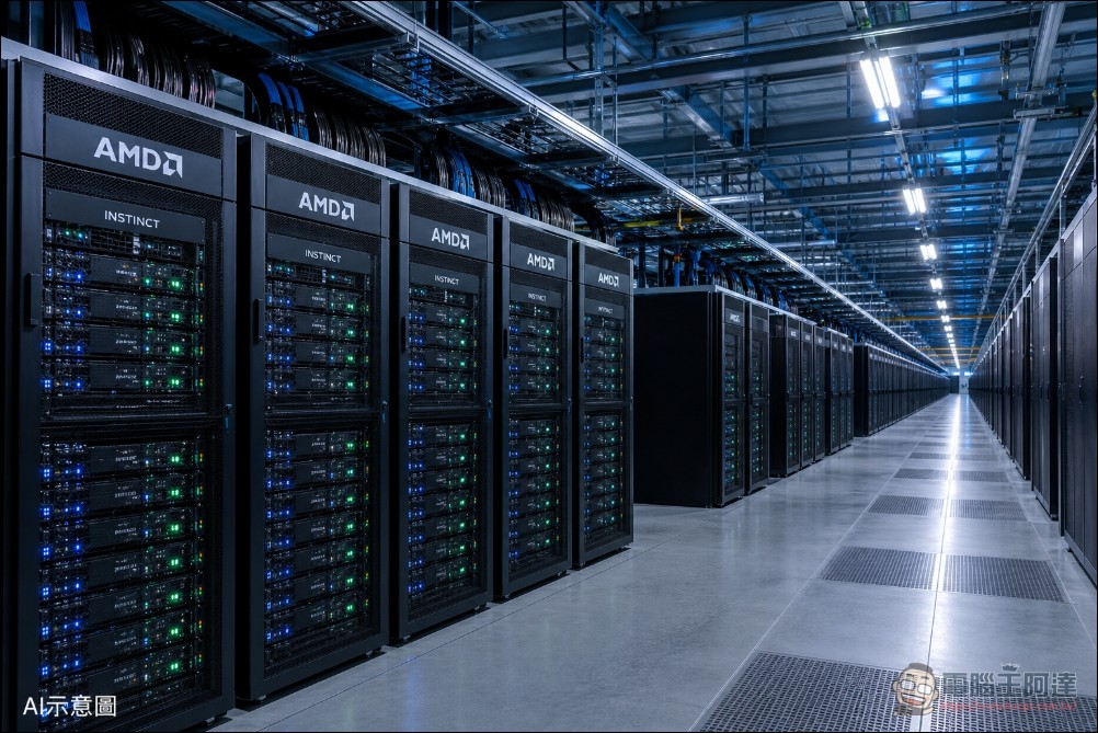
According to previously announced specifications at CES 2026, each Helios rack can carry up to 72 MI450 series GPUs, providing up to 2.9 exaFLOPS AI computing performance, equipped with 31TB of HBM4 memoryand 260TB/s interconnect bandwidth. These numbers mean that a single Helios rack has enough computing power to train the largest trillion-parameter AI model currently available.
In terms of ODM cooperation,Sanmina, Wiwynn, Wistron and Inventec are manufacturing partners of Helios systems. Both Wiwynn and Inventec stated that their cooperation aims to provide a complete integrated solution with high performance and high reliability for ultra-large-scale data centers. In addition, AIC Corporation (AIC) also participated in the Helios project and was responsible for the structural design of rack-level and computing trays.
Key supply chain layouts in the AI arms race
The timing of AMD’s tens-billion-dollar investment is quite intriguing. Just a few months ago, Nvidia announced an agreement with TSMC to lock in a large amount of CoWoS packaging capacity, and it was rumored to pay TSMC billions of dollars in advance payments to ensure mass production of Blackwell and Rubin architectures (CNBC, 2026/4/8). Now AMD is directly entering the upstream of packaging production capacity with a larger investment scale, obviously to ensure supply chain autonomy in the AI chip war.
For Taiwan’s semiconductor industry chain, the direct effect of this investment will be considerable. Packaging and testing factories such as ASE, Silicon Products, and Licheng will receive mass production orders for EFB technology, and carrier board factories such as Xinxing, Nanya Circuit Board, and Jingshuo will also benefit from the increased demand. This also echoes the Taiwanese government’s previously announced tens of billions of dollars in AI national investment plans, and a complete closed loop from policy to industrial chain is taking shape.
At a time when the construction of global AI infrastructure is still in a stage of rapid expansion, AMD’s tens of billions of dollars in Taiwan bet is not only a supply chain layout, but also a head-on challenge to Nvidia’s dominance in the AI accelerator market. As the Venice CPU, MI450X GPU and Helios platform will be in place in the second half of 2026, whether AMD can truly shake Nvidia’s dominance will be the most noteworthy front in the AI semiconductor industry in the next two years.
Source: KOCPC Chinese