


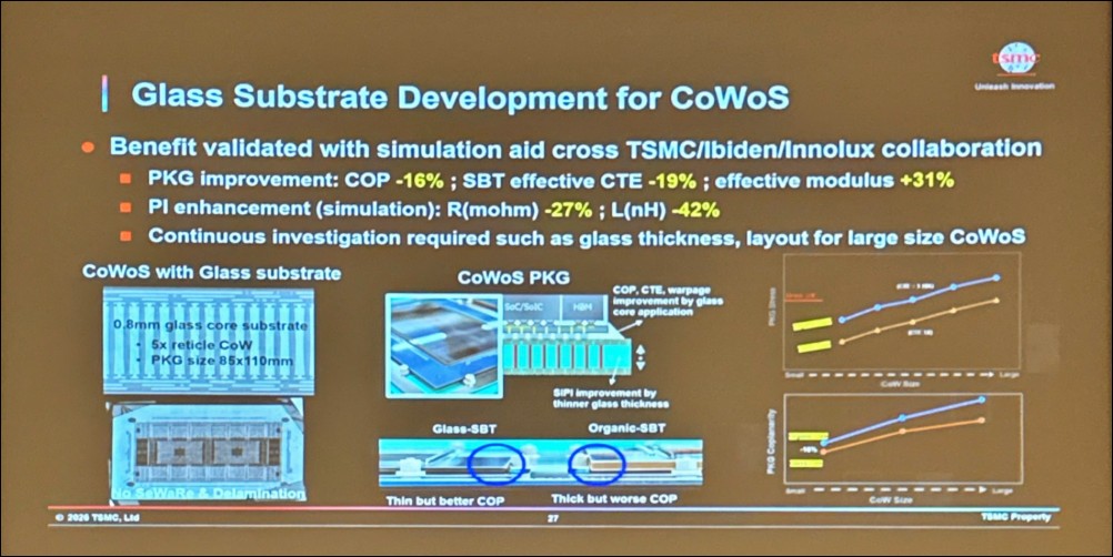
Tianfeng International analyst Ming-Chi Kuo published a long article on X on the 18th, providing an in-depth interpretation of a leaked slide from TSMC’s JPCA Show 2026 briefing in Japan on June 11. The slideshow is titled “Glass Substrate Development for CoWoS” and reveals that TSMC has joined hands with Japanese substrate manufacturer Ibiden and Taiwanese panel manufacturer Innolux to jointly develop a glass core substrate, with the goal of entering mass production from the fourth quarter of 2028 to the first quarter of 2029.
重點解讀台積電的玻璃核心載板投影片
台積電在 6 月 11 日的日本 JPCA Show 2026,進行主題為「AIの進化に不可欠な先端パッケージング技術」的簡報,該份簡報約40頁,當中某張標題為「Glass Substrate Development for CoWoS」的投影片流出,引發廣泛關注。… pic.twitter.com/l8GD7MwN72
— 郭明錤|Ming-Chi Kuo (@mingchikuo) June 18, 2026
The two major technical pillars under the CoPoS architecture: oS and CoP
To understand the significance of this slide, we must first clarify the architecture of TSMC’s next-generation packaging platform CoPoS (Chip-on-Panel-on-Substrate). CoPoS is TSMC’s next-generation advanced packaging technology after the existing CoWoS. The core concept is to convert the packaging substrate from circular wafers to square panels, thereby breaking through the area and cost bottlenecks faced by CoWoS.
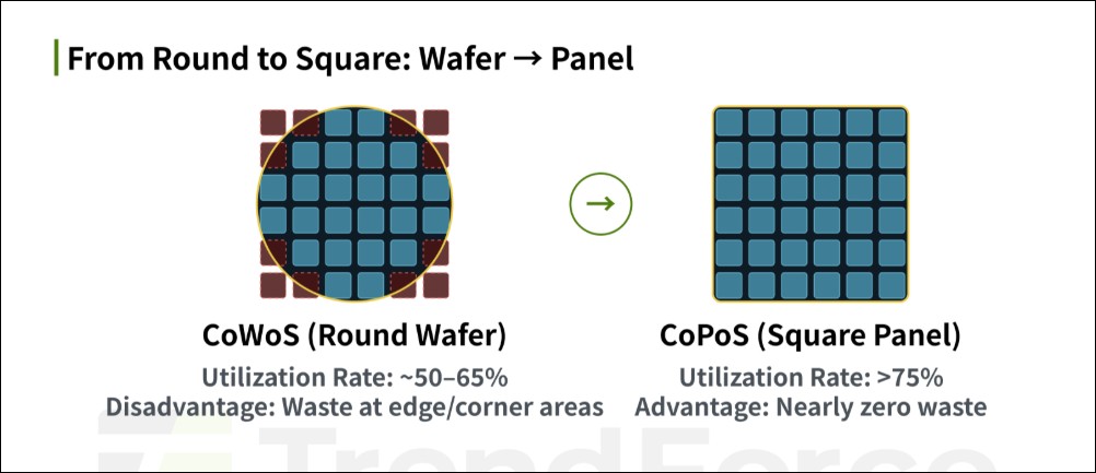
CoPoS can be broken down into two key technical links:
- oS(on Substrate): The glass core carrier board is used to replace the traditional ABF organic carrier board to solve the problem of warpage and durability of the chip. Ming-Chi Kuo pointed out that this involves “whether the chip can be made and whether the chip can operate.”
- CoP(Chip-on-Panel): The panel-level packaging process solves the problems of production efficiency and cutting economy, which is directly related to cost and selling price.
Ming-Chi Kuo’s key judgment is that the market underestimates the importance of glass core carrier boards. In the CoPoS architecture, the technical positioning of oS is higher than that of CoP. He further pointed out that CoP is “very-nice-to-have”, and the cost of not having it is that the chips are more expensive; but oS is “must-have”, and without this technology, “it may even be a problem whether we can make usable chips.”
This also explains why TSMC first matched the glass core carrier board with the existing CoW (Chip-on-Wafer) instead of CoP during testing. CoW is a test vehicle capable of validating the most challenging mechanical structural issues when using composite materials. The good test results mean that TSMC, Ibiden and Innolux have broken through key technical bottlenecks.
The core data of the slide show: power integrity improvement is where the gold lies
Ming-Chi Kuo believes that the “most valuable” part of this slide is the improvement data on power integrity (Power Integrity, PI). The technical logic chain is as follows:
- Glass core carriers are thinner than traditional ABF carriers
- Thinner carriers enable shorter vertical conduction paths for TGV (Through Glass Via)
- The conduction path is shortened, causing the resistance (R) and loop inductance (L) to decrease simultaneously.
- R and L drops directly improve power integrity
According to supply chain survey data, the parameters of TSMC’s glass substrate test samples have been improved as follows: warpage is reduced by 16%, thermal expansion coefficient is reduced by 19%, resistance is reduced by 27%, and inductance is reduced by 42%. Among them, the inductance dropped by 42%, which has the most profound significance for AI chips.
Why does PI improvement matter to customers? Ming-Chi Kuo’s derivation is that improved PI means more stable power supply, thereby releasing power headroom. These margins allow chip designers to integrate more transistors or increase the operating clock, which ultimately translates into a direct increase in the computing power of AI chips.
For customers like Nvidia, production efficiency is TSMC’s “basic responsibility” and customers will not pay extra for it. However, improvements in AI computing power can directly translate into customers’ competitiveness and profits, so customers are willing to pay for the high unit price of glass carrier boards. Ming-Chi Kuo also revealed that in addition to Nvidia, two American customers have expressed high interest in glass core carrier boards.
Cost structure analysis: high unit price does not affect customers’ willingness to adopt
The unit price of glass core carrier boards is several times higher than that of existing ABF carrier boards. Among them, the unit price of glass processed by Innolux is “very high” and is the most core material. However, Ming-Chi Kuo believes that high unit price will not be an obstacle to customer adoption for two reasons:
- Currently, the cost of carrier boards accounts for a low single-digit percentage of the BOM (bill of materials) of AI chips. Even if the cost of glass carrier boards in the future is several times higher than the current cost, the proportion of the BOM will still be low.
- The loss caused by packaging yield is about 5 to 10 times the cost of the carrier board. Glass carrier board can improve packaging yield, which is equivalent to indirectly reducing greater hidden costs.
In other words, glass substrate is both a “cost reduction tool” (increasing yield and reducing packaging losses) and a “price increase bargaining chip” (increasing AI computing power and making customers willing to pay higher prices), which is a positive addition to TSMC’s profits and competitive advantages.
Technical details: TGV is core Know-how, TSMC refuses to answer
During the Q&A session after the briefing, an audience member asked about the TGV details of glass core carrier boards, but TSMC refused to answer on the spot. Ming-Chi Kuo pointed out that the key technology for glass core carrier boards is TGV, and the core know-how is currently in the hands of TSMC and Innolux. In contrast, another questioner asked about the integration of IVR, eDTC and LSI, and TSMC answered a lot.[1]
TGV is a technology that drills tiny via holes on a glass substrate and then fills them with conductive material to achieve vertical electrical connections. Since glass itself is not conductive, the quality of the TGV directly determines the electrical performance of the carrier board. This is why TSMC regards TGV as a core secret and is unwilling to disclose any details in public.
Mass production schedule and supply chain layout
According to Ming-Chi Kuo’s industry survey, the glass core carrier board in the slide is cut from a size of 250×250mm. The ABF layer is mainly made of Ajinomoto’s GL107 material, mixed with ABF-GCP, and tested with 24 to 28 layers of the mainstream AI chip ABF specifications from 2027 to 2028.
Ibiden is currently responsible for cutting 250×250mm glass core carrier boards. When the 510×515mm size is used for pre-mass production simulation in the second half of 2027, if Ibiden still wants to reduce production complexity to maintain its ultra-high gross profit margin, Innolux, which is more familiar with the characteristics of glass, may be responsible for cutting.
In terms of timetable, TSMC aims to start mass production of glass core carrier boards from the fourth quarter of 2028 to the first quarter of 2029 to match the iteration rhythm of Nvidia AI chips. TSMC expects to build the first CoPoS experimental line in Caiyu (6789) in 2026, and the mass production base will be located in the P4 and P5 factories of Chiayi AP7 Factory.
Ibiden’s conservative roadmap vs TSMC’s aggressive timeline
Ming-Chi Kuo also interpreted the statement in Ibiden’s slideshow that the glass core carrier board schedule is listed as CY30 (2030). He believes that this means that “Ibiden, which has always been conservative and cautious externally, has officially listed glass core carrier boards as a development route”, which in turn confirms the long-term trend of this technology.
However, Ming-Chi Kuo also reminded that some details of Ibiden’s slides are not completely consistent with market information. For example, the reticle schedule is about one generation different from what TSMC has publicly announced, and the Rubin Ultra carrier board size is significantly larger than the 90×90mm marked by Ibiden in CY26-27, etc. “This illustrates the need for cross-verification from multiple parties at any time when predicting the future,” Ming-Chi Kuo wrote.
Industrial competition landscape: South Korea’s supply chain is under pressure
TSMC’s progress in the field of glass substrates also affects the competitive situation of the global supply chain. According to Chosun Bizreport, Korean suppliers are at risk of falling behind as TSMC’s glass core carrier board CoWoS test results show significant improvements in reliability. Absolics, a subsidiary of SKC, is also an active player in the field of glass substrates, but TSMC’s choice to cooperate with Ibiden and Innolux is equivalent to making a clear supplier choice on the technical route.
In addition, TSMC explained COP in the briefing as Coplanarity (flatness/coplanarity) instead of the common abbreviation of Chip-on-Package in the industry, which also reflects the uniqueness of the terminology definition of CoPoS technology.
Conclusion: Glass substrate is the next battlefield for AI chips
From CoWoS to CoPoS, from organic carrier boards to glass core carrier boards, TSMC is paving the way for the next generation of AI chip packaging architecture. Ming-Chi Kuo’s interpretation clearly divided the technical priorities of oS and CoP, and also pointed out the dual value of glass substrates to TSMC: both reducing packaging costs and increasing chip selling prices.
For Taiwan’s semiconductor supply chain, Innolux’s changing role from panel factory to glass substrate material supply, as well as the trend of 13 Taiwanese manufacturers entering the CoPoS supply chain, indicate that advanced packaging will be one of the industry tracks with the most growth potential in the next few years.
Source: KOCPC Chinese