


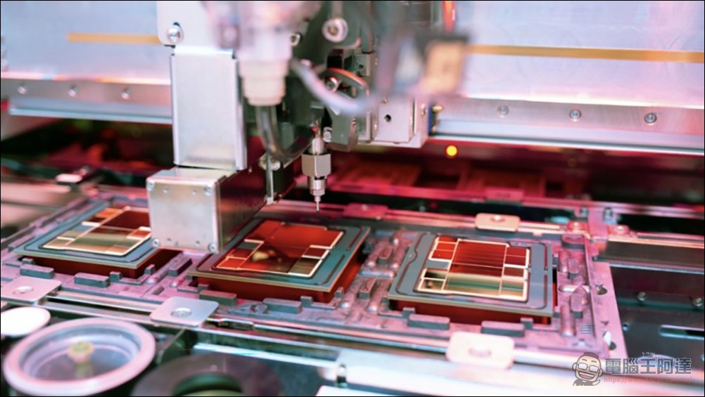
At IEEE 2026 Electronic Components and Technology Conference (ECTC), Intel unveiled next-generation packaging solutions EMIB-T, formally to TSMC CoWoS Challenged. The biggest highlight of this technology is integrating TSV (through-silicon via) into EMIB’s silicon bridge, allowing current to pass vertically through the substrate directly to the chip, completely solving the power delivery bottleneck.
Intel EMIB-T Packaging Debuts: HBM4e Hits 12 Gb/s, Costs 40% Less Than CoWoS
EMIB-T announced several key developments at ECTC 2026:
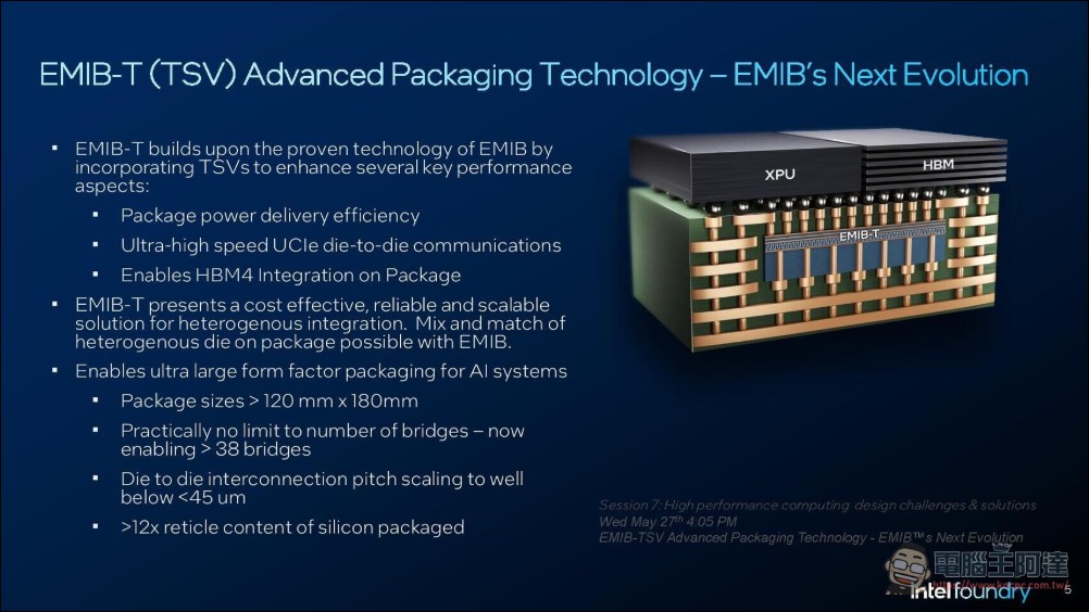
- First-level interconnect bump pitch scaled down to 25μm, with package dimensions expanded to 120×120mm
- Compute and storage chips integrated in a single package exceeding 9x reticle area, with actual chip count surpassing the 10x reticle threshold
- Co-optimizing signal and power delivery integrity, HBM4e achieves 12 Gb/s data rates while the UCIe interface reaches 64 Gb/s.
Intel Vice President Rahul Manepalli said EMIB-T will retain the current EMIB’s energy efficiency of approximately 0.25pJ/bit and further improve interconnect density.
EMIB-T Core Technology: Switching power delivery from “detour routing” to “through-package routing”
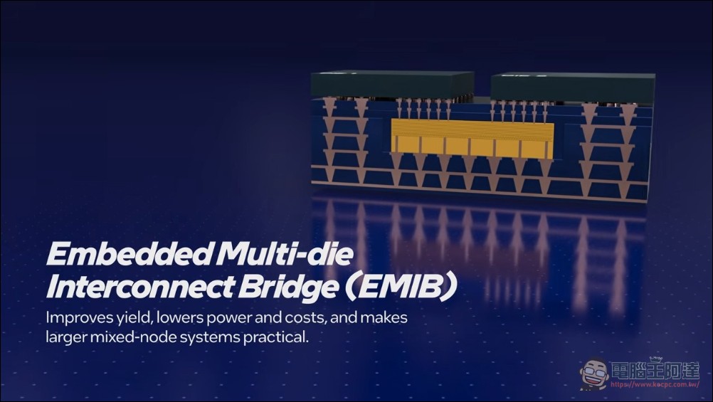
Traditional EMIB (Embedded Multi-die Interconnect Bridge) uses embedded silicon bridges to achieve high-density interconnects locally, but power must be routed around the silicon bridge, resulting in long power delivery paths and high losses, which can easily cause voltage drop when dealing with high-bandwidth memory like HBM4e.
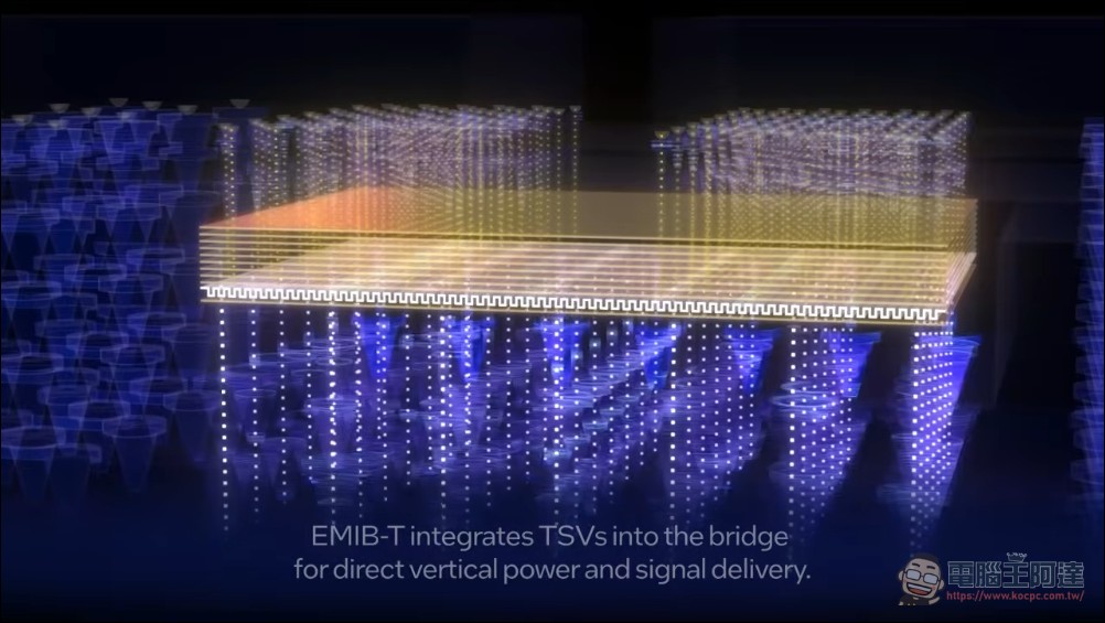
The EMIB-T solution integrates TSV (Through-Silicon Via) and MIM (Metal-Insulator-Metal) capacitors within the silicon bridge, allowing both power and signals to pass directly through the silicon bridge vertically. Current flows straight through the substrate to reach the chip, significantly shortening the power delivery path and increasing power delivery density. If EMIB is the bridge connecting chiplets, EMIB-T is a three-dimensional interchange ramp.
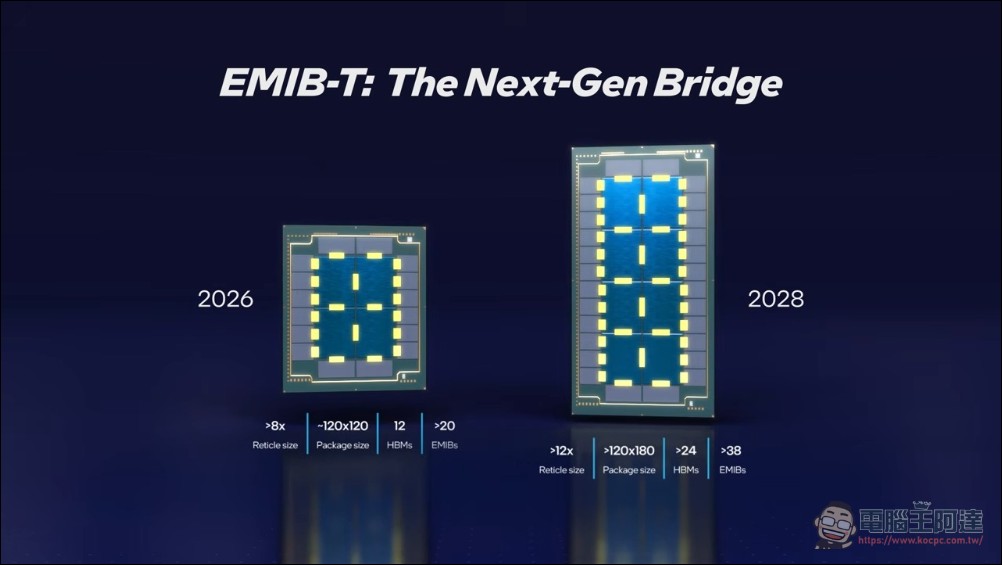
Specifications scaled up across the board: 120×120mm package, 9x mask, 20 bridge connectors
According to Intel’s official data, EMIB-T has been implemented in packages larger than 120×120mm, accommodating more than 9× the die area of silicon, including 12 HBM modules, 4 dense chiplets, and over 20 bridges; the first-layer interconnect bump pitch has been reduced to 25μm.
Intel also showcased three extended technologies:
- 3D SRAM Chiplet IntegrationUsing a fan-out embedded bridge platform, a 50:50 read/write workload achieves a bandwidth density of 265 GB/s/mm², with energy consumption below 0.24 pJ/bit, dropping to 0.15 pJ/bit at lower frequencies.
- Extra-large HLFF packageEMIB-T has the potential to scale to 240×240mm ultra-large-format packaging, enabling integration of ASIC, HBM, I/O and other chips, with material and process innovations overcoming flow distance and void challenges during the molding of ultra-large chip assemblies.
- Signal and Power Integrity OptimizationIntel data shows that at 12Gb/s speed, the eye diagram width is approximately 67% (with DFE equalization).
Intel plans to produce 120×120mm EMIB packaging substrates starting in 2026, which will be expanded to 120×180mm in the future, capable of accommodating over 24 HBM stacks, 8 compute chiplets, and more than 38 EMIB bridges.
Compared to TSMC’s CoWoS: 40% Lower Cost, Yield Exceeding 90%
CoWoS places all chips on a large-area silicon interposer, with package size strictly limited by the reticle limit. EMIB uses localized silicon bridges embedded in an organic substrate, bridging only where interconnects are needed. The tiny silicon bridges can be densely arranged on the wafer, achieving nearly 100% material utilization. After removing the large-area interposer, packaging costs are reduced by over 40% compared to CoWoS. In terms of yield, EMIB-T has broken through 90%, reaching industry-leading levels. Intel states that EMIB offers advantages in cost, scalability, and performance, with performance sufficient to rival more advanced SoW (Silicon-on-Wafer) technologies.
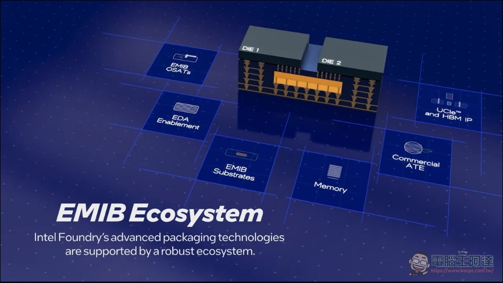
Intel emphasizes that the key advantage of EMIB-T lies in its IP and process node-agnostic nature, allowing customers to freely package together chips manufactured using different architectures, various third-party fabs, or Intel’s own internal process nodes, which simplifies supply chain management.
Customer list takes shape: Google TPU, MediaTek follow suit
Google’s next-generation TPU has decided to abandon TSMC’s CoWoS and switch to Intel’s EMIB-T. MediaTek announced at COMPUTEX 2026 that its next-generation chips will exclusively use EMIB-T. Google plans to adopt EMIB packaging for the TPU v9 in 2027, with MediaTek taking on the design work. Google is also considering bypassing MediaTek and sending chip designs directly to TSMC to save costs, but Intel would still handle the packaging stage.
MediaTek’s partnership with Intel has extended to a new Taiwanese supply chain, with PSMC and AP Memory joining the Google TPU supply chain. AP Memory’s SiCap (silicon capacitor) products play a key role in MediaTek’s Google AI chip design, and with SiCap production capacity expected to reach 10,000 units per month by end of 2027, PSMC may play a significant role in capacity expansion.
According to Tom’s Hardware, EMIB-T is expected to enter pilot production before the end of this year. Intel has also unveiled a new heatsink design that can reduce voids in thermal interface materials by approximately 25%, and introduced a new thermal compression bonding process to reduce warpage in large-format package substrates.
The End of CoWoS’s Monopoly Era?
After the AI boom, CoWoS became a scarce bottleneck resource for the industry, with TSMC’s capacity in long-term undersupply. Intel’s EMIB-T offers a different approach: bridging chips on small silicon bridges to avoid the cost and size limitations of large-area silicon interposer. On the progress front, Intel presented 12 papers at ECTC 2026 targeting CoWoS, advancing simultaneously across four major areas: power integrity, signal integrity, thermal management, and materials. The 2028 roadmap to expand packaging to 120×180mm and integrate over 24 HBM stacks signals that advanced packaging is evolving from chip interconnection toward system-level integration.
However, there are still variables in the commercialization of EMIB-T. Orders from Google and MediaTek ultimately depend on Intel’s actual production yields. Major customers like Apple, AMD, and NVIDIA have reportedly been in contact but haven’t made any public commitments. When Intel’s own 18A process reaches industry-standard yields is also a key factor for whether EMIB-T can move forward smoothly. TSMC isn’t standing still with CoWoS either—CoPoS, with its larger area and higher utilization, is also on the way. Who will ultimately win this advanced packaging battle remains to be seen.
Source: KOCPC Chinese