


The well-known Chinese tech channel Geekerwan, in its latest video, tears down and reviews the latest Apple A20 Pro chip used in the iPhone 18 Pro and 18 Pro Max. The core conclusion is that the iPhone 18 Pro series has little change in exterior design (new color options and a smaller Dynamic Island), but internally it has been comprehensively overhauled, from chip packaging, CPU microarchitecture, GPU, and NPU to the cooling system. The A20 Pro chip also delivers Apple’s biggest performance and efficiency leap in five years.
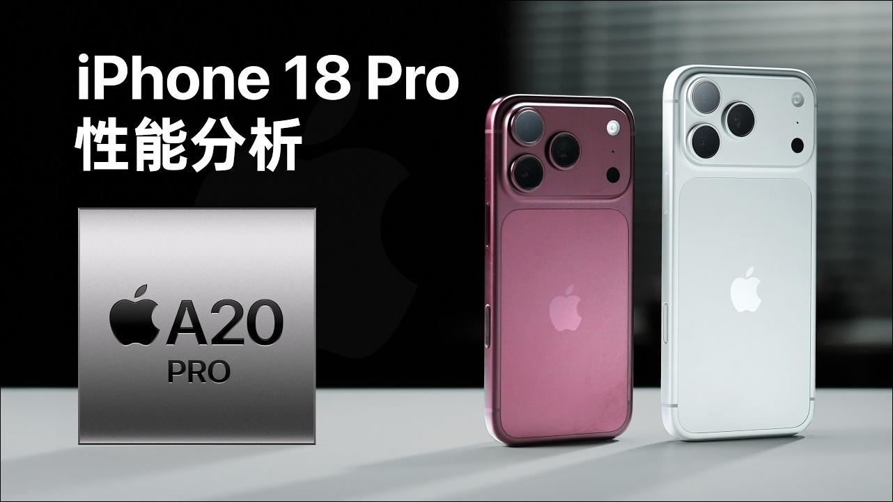
Apple A20 Pro chip teardown analysis
Secret One: WMCM packaging, memory moves away from above the chip.
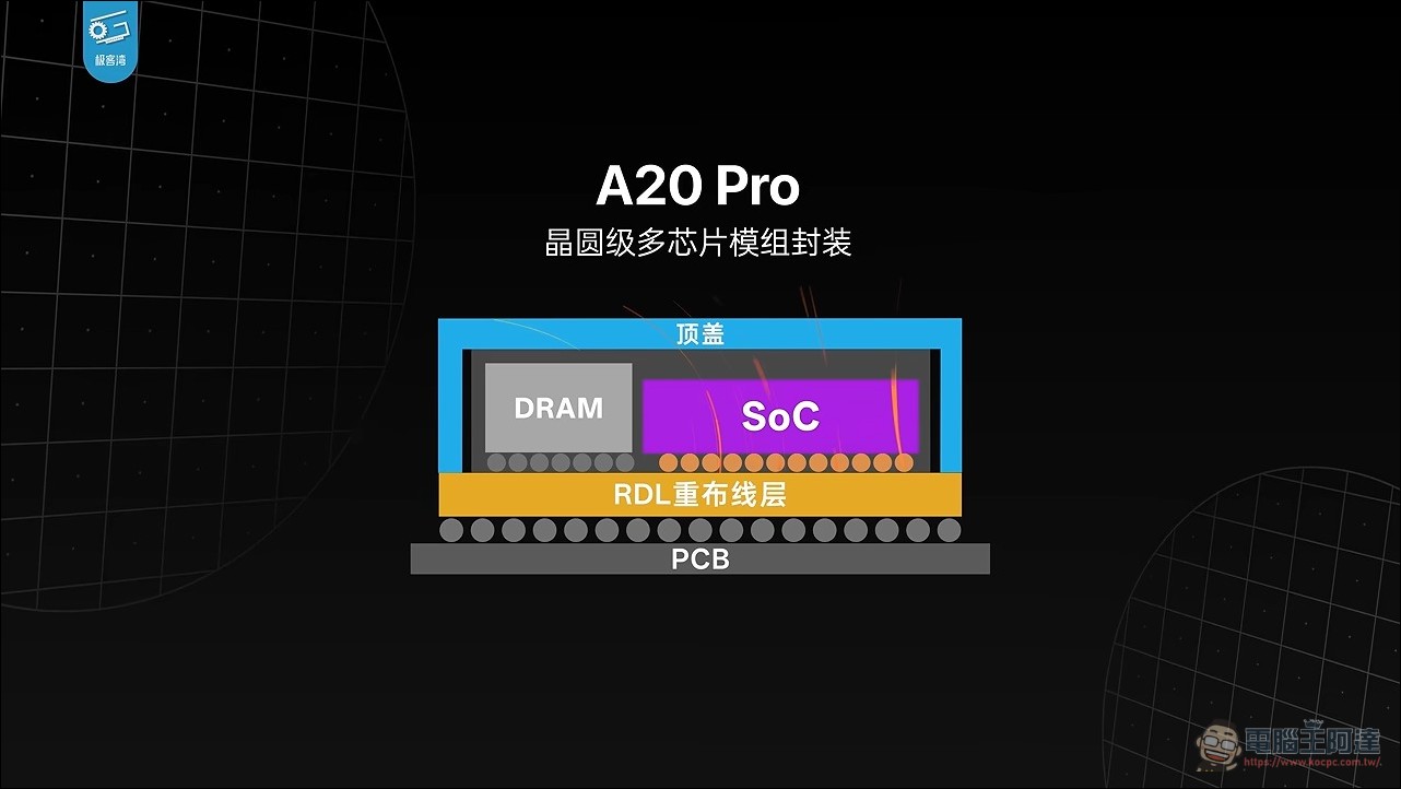
The biggest structural change in the A20 Pro is its packaging technology. Traditional smartphone chips use PoP (Package on Package) packaging, with memory stacked on top of the processor. This design, over 20 years old, was intended to save space, but as chip power consumption continues to climb, having memory stuck on top severely hinders heat dissipation.
Apple is switching to WMCM (Wafer-Level Multi-Chip Module) packaging, integrating the chip and memory side by side into a single module, with a heat spreader added on top. This technology was inspired by Apple’s own M-series computer chips, but the approach differs: the M series places the chip and memory side by side on a package substrate, while the A20 Pro completes the integration at the wafer level.
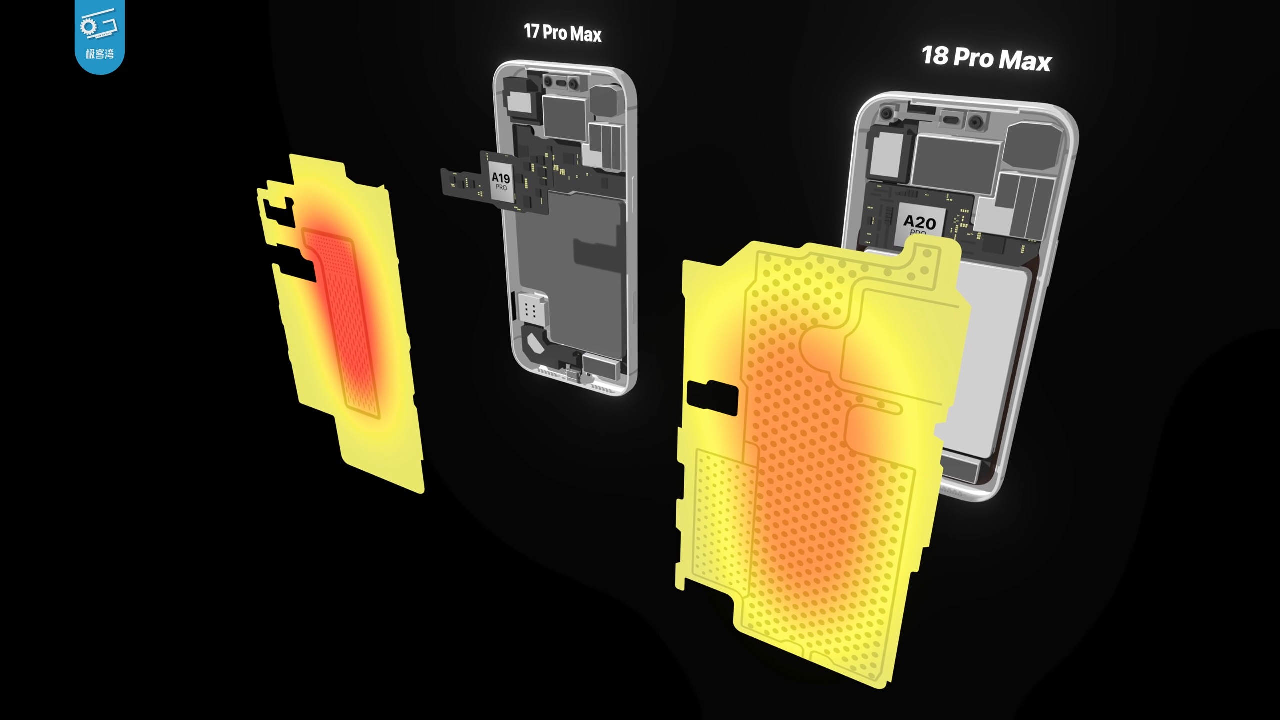
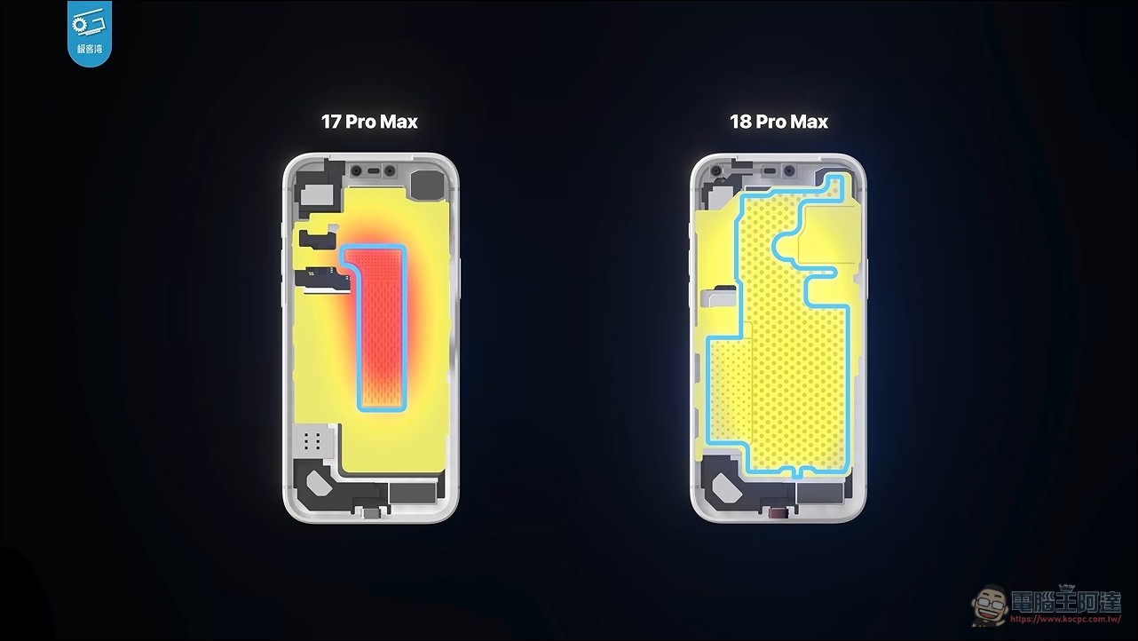
Beyond the packaging, the iPhone 18 Pro’s motherboard layout has also been completely redesigned. The A20 Pro sits directly on the outer side of the motherboard, making direct contact with a vapor chamber that is 3 times the area of the previous generation—larger than many Android performance flagships.
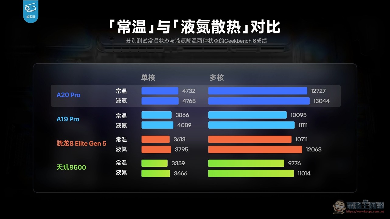
The core value of WMCM packaging lies in solving the problem of whether high clock speeds can actually be used. In the past, even if a chip could reach close to 5GHz, it was difficult to maintain peak clock speeds at room temperature. Geekerwan testing found that the iPhone 18 Pro’s Geekbench scores were almost identical at room temperature and in extremely low-temperature environments, meaning the A20 Pro can stably run at its full 4.93GHz at room temperature.
Secret Two: TSMC’s N2 process has limited density gains but higher clock speeds.
The A20 Pro uses TSMC’s N2 process, moving from FinFET to GAA (gate-all-around) transistors. However, Geekerwan points out that the first generation of N2 has limited density improvements: the high-density library barely beats N3P, while the high-performance library actually has lower density. Apple chose N2 over N2P (competitors are adopting N2P this year), with the main gain being higher clock capability rather than a density dividend.
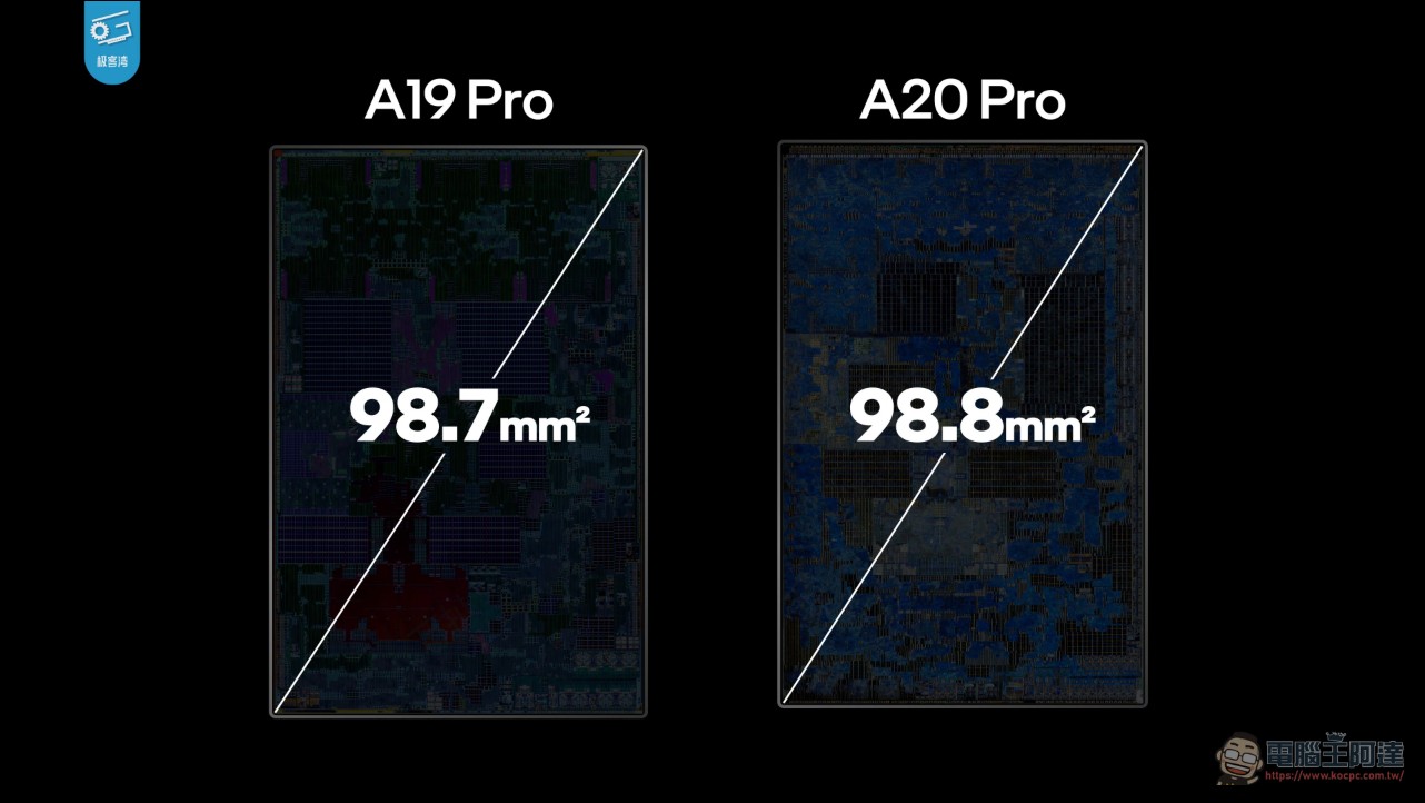
This is an interesting decision. N2P offers further density improvements, but Apple chose first-generation N2, possibly because WMCM packaging has already solved the thermal issue at the system level, so it doesn’t need to rely on process density to gain more space.
Secret Three: All-New S-Core, Apple Shrinks Its Flagship Core for the First Time
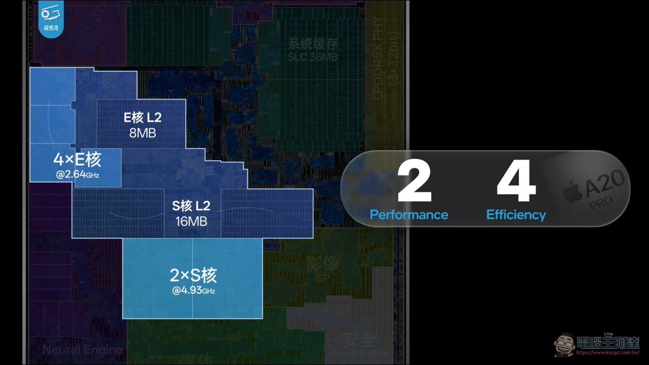
The A20 Pro’s CPU retains a configuration of 2 high-performance cores plus 4 efficiency cores, but Apple has renamed the high-performance cores from “P-core” to “S-core” (Super core), because the original P-core name was given to the new desktop-class cores.
The most surprising change is at the microarchitecture level: this all-new S-core is smaller than the previous generation. The front-end decoder is reduced from 10-wide to 9-wide, and the capacities of the register file, out-of-order scheduling queue, and integer/floating-point schedulers are all reduced to varying degrees. But the number of back-end execution units is unchanged, and the L1 cache size is also unchanged. The result: at a 4.93GHz peak clock, integer IPC actually improves by 3%.
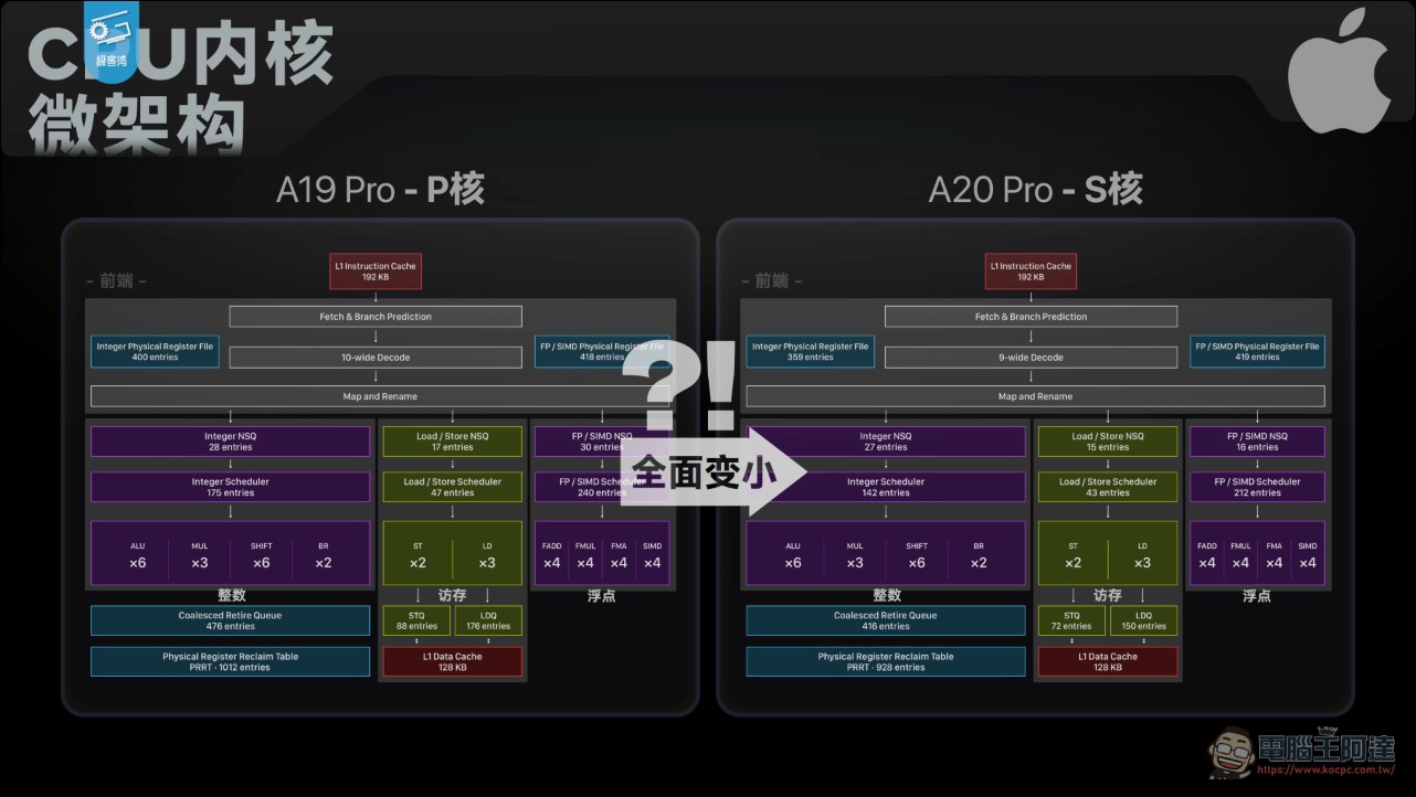
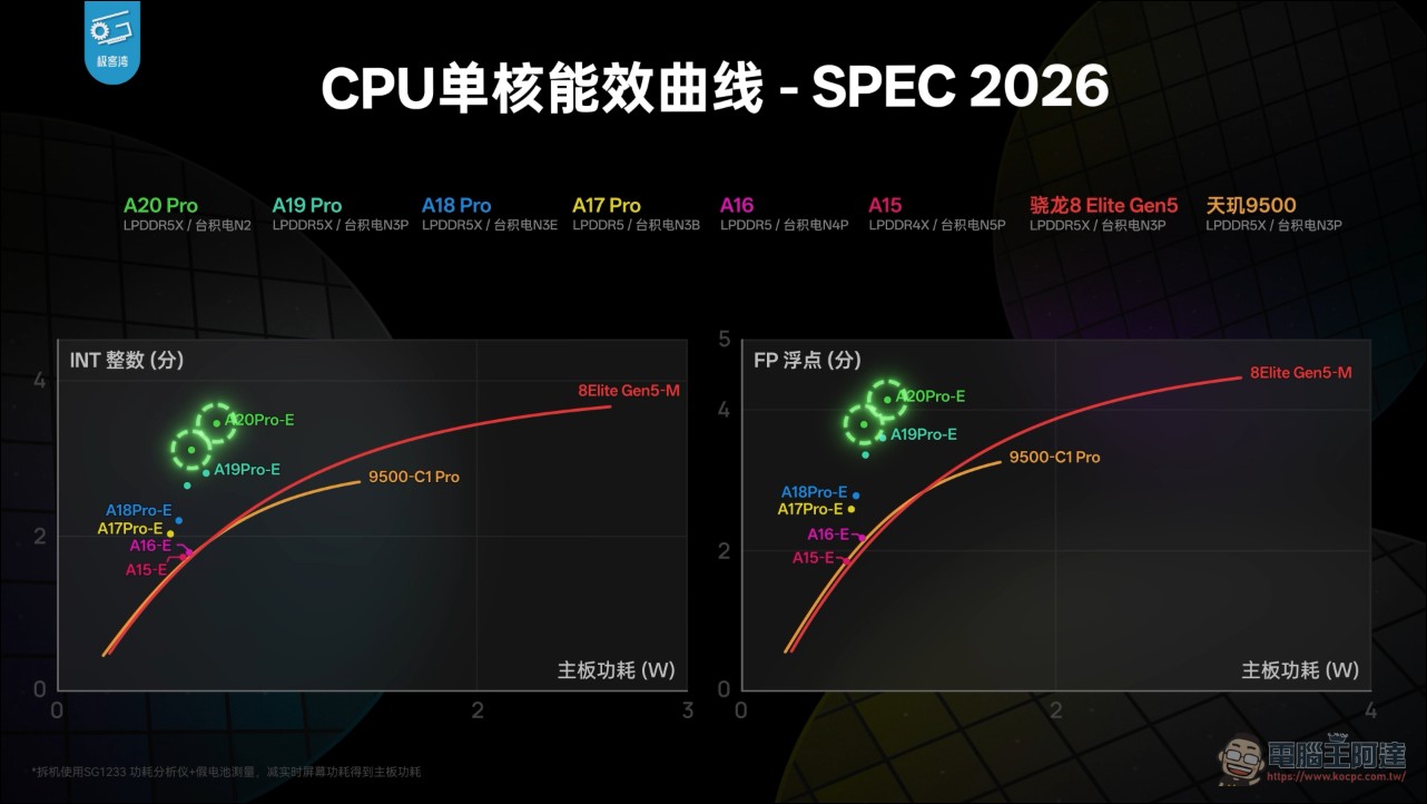
Geekerwan bluntly stated, “I’ve never seen an Apple flagship core shrink.” Apple’s strategy in the past was to make each generation’s core larger. This time it went the opposite way: using a more streamlined core in exchange for higher clock speeds while maintaining per-clock performance. This is a completely new design approach, entirely different from Apple in the past.
E-Core is equally impressive, with efficiency catching up to Qualcomm’s mid-core.
The upgrade to the E-core is just as surprising. Peak clock speed rose slightly from 2.59GHz to 2.64GHz, power consumption remained almost unchanged, but performance improved significantly. The peak performance of the A20 Pro E-core is close to the mid-core of the Snapdragon 8 Elite Gen 5, but Qualcomm needs 2.6W while Apple uses less than 0.8W, only one-third the power consumption.
Microarchitecture changes include: L1 instruction cache increased from 128KB to 160KB, L1 data cache from 64KB to 96KB, integer multipliers from 1 to 2, integer scheduler capacity from 33 to 47 entries, buffer queue from 14 to 20, plus an 8MB shared L2 cache. These changes each target a bottleneck in the previous generation’s design.
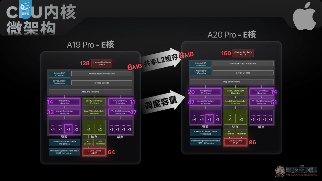
The E-core in the A19 Pro had just undergone a major architectural overhaul (a full 6-wide decoder), and the A20 Pro brings an upgrade of comparable scale. Apple’s CPU design team has achieved two E-core leaps in two consecutive years, which is extremely rare in the industry.
Memory bandwidth surges 50%, with latency rivaling desktop PCs.
The A20 Pro’s memory controller has been upgraded from 64-bit LPDDR5X to 96-bit LPDDR5X. Because LPDDR5X lacks error checking bits, its memory bandwidth even surpasses that of 96-bit LPDDR6-10667 with the same bus width, reaching 115.2GB/s, a 50% surge over the previous generation and approaching M4 levels.
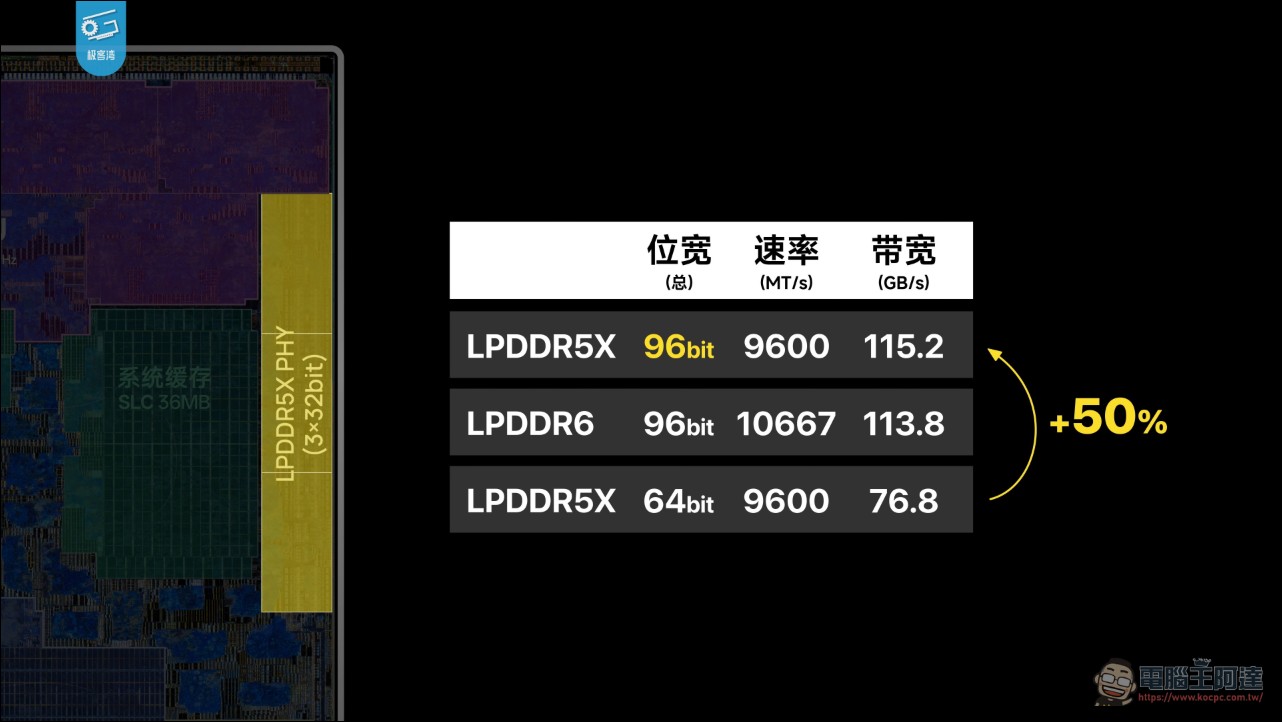
Geekerwan also pointed out that memory latency, which Apple did not mention at the launch event, has improved significantly. The S-core’s memory latency is only 70ns, on par with desktop CPUs equipped with DDR5; the E-core’s latency is also only 100ns, lower than the high-performance cores of many chips.
GPU performance jumps 40% with no increase in power consumption.
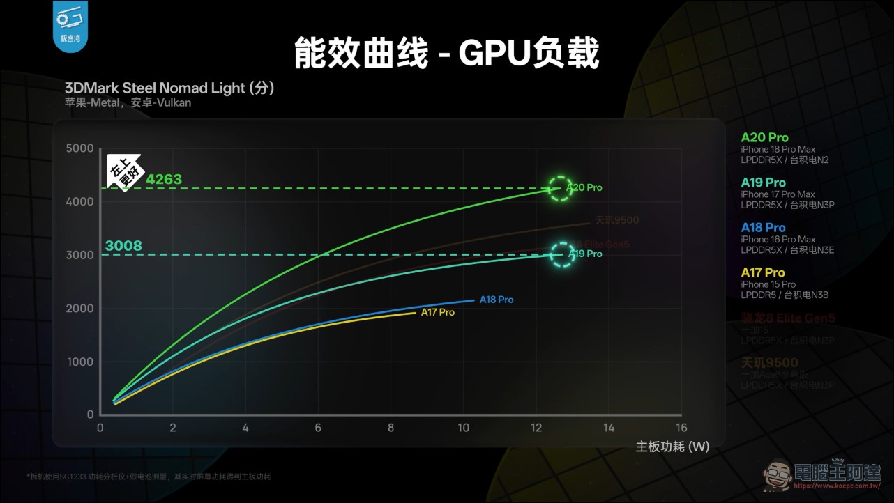
The GPU was upgraded to the Family 11 architecture, with the core count increasing from 6 to 7, marking Apple’s first increase in GPU core count since the A17 Pro. In the 3DMark Steel Nomad Light test, the A20 Pro’s peak GPU score jumped from the previous generation’s 3,008 to 4,263, surpassing Apple’s officially claimed 40%, and this 40% performance improvement comes with no increase in power consumption.
FP32 compute has increased from 2.4 TFLOPS to 2.8 TFLOPS. The new architecture also introduces a Neural Accelerator (similar to Tensor Core), improving the efficiency of frame interpolation and super-resolution while also accelerating prefill operations for large AI models.
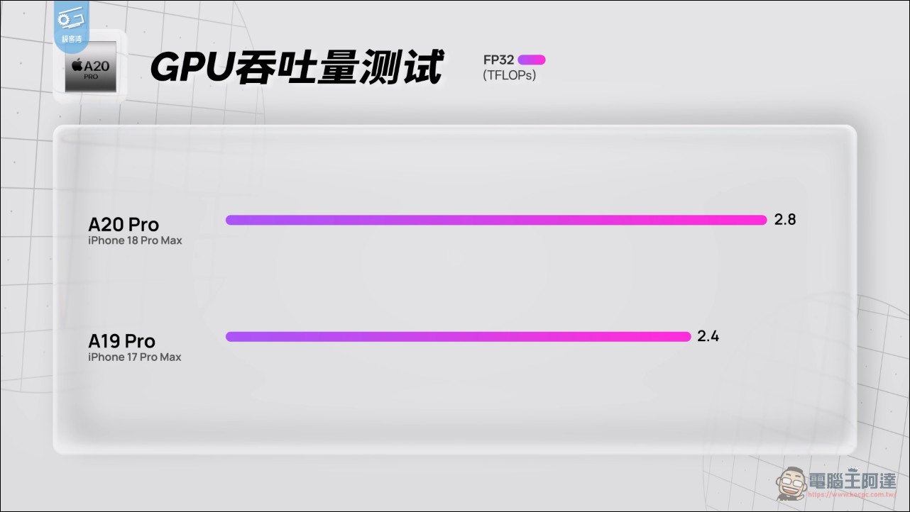
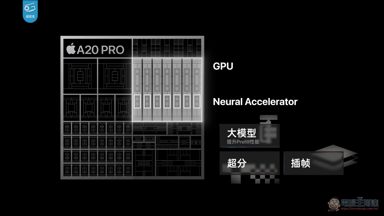
Geekerwan believes this is Apple’s biggest GPU leap since the A15. Memory bandwidth has always been the main bottleneck for mobile GPUs, and the A20 Pro’s 50% bandwidth increase in one go directly unlocked the GPU’s potential.
NPU doubled to 32 cores, INT8 reaches 73 TOPS
The NPU doubled from 16 cores to 32 cores, and its share of chip area surged by 60%. Geekerwan’s testing: the A19 Pro peaks at 24 TOPS at FP16 precision and 41 TOPS at INT8 (higher than Apple’s claimed 35 TOPS); the A20 Pro reaches 44 TOPS at FP16 and 73 TOPS at INT8.
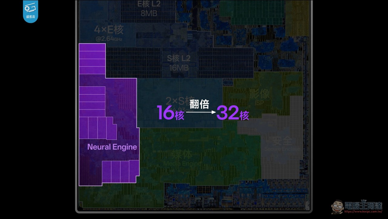
In terms of chip area allocation, the proportions for the CPU and GPU are both smaller than in the previous generation, while only the NPU has expanded significantly. Apple’s investment direction for the NPU is very clear: on-device AI inference is the core battleground of the future.
Cooling catches up to gaming phones, vapor chamber area 3x the size.
The iPhone 18 Pro series has a vapor chamber area 3 times that of the previous generation. Geekerwan used the OnePlus 15 and iQOO 15 Ultra (with a built-in fan) as control groups for a 20-minute stress test. The results show that the front surface temperature of the 4 iPhones stabilized at 44-45°C, and the power consumption they could sustain at this temperature was comparable to that of the OnePlus 15 at 47°C and the iQOO 15 Ultra at 46°C.
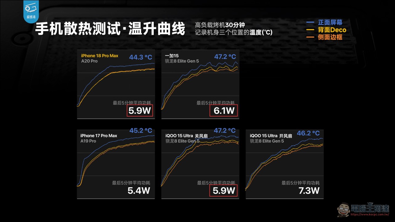
Geekerwan commented, “The iPhone’s cooling has caught up from lagging behind a few years ago to keeping pace with Android performance flagships.” However, it still can’t fully match the iQOO 15 Ultra with its fan at full speed.
Gameplay test: Genshin Impact at 3.4W, Surface temperature not exceeding 39°C
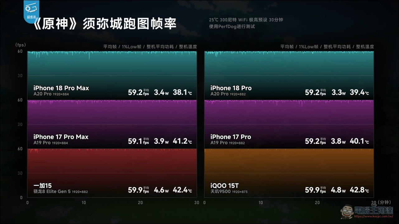
In the Genshin Impact 60fps (884p) test, the iPhone 18 Pro Max’s total device power consumption was only 3.4W, while the smaller 18 Pro was even lower at 3.3W. Android flagships (Snapdragon 8 Elite Gen 5, Dimensity 9500) consume between 4.6-4.8W, and the previous-generation iPhone 17 Pro Max was 3.9W. After subtracting 0.6W for the display and network, the A20 Pro’s compute power consumption is 15% lower than the previous generation. Surface temperature is only 38-39°C.
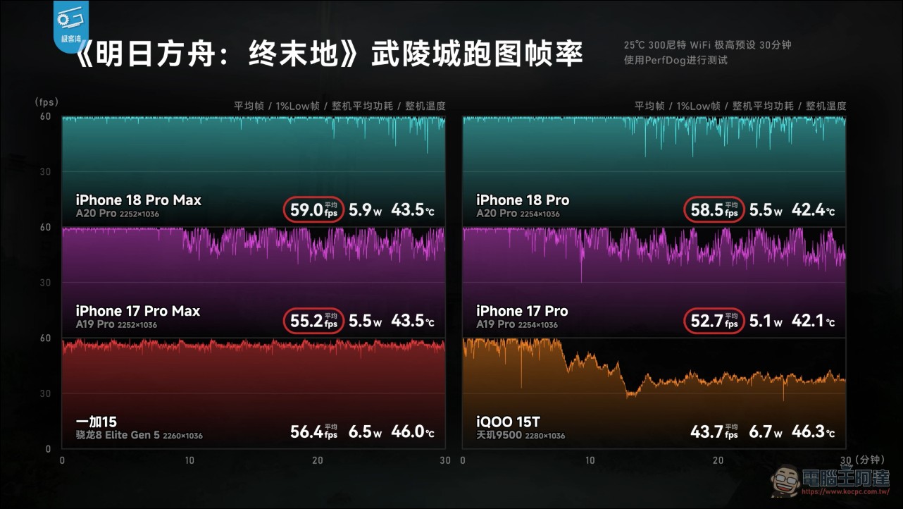
In a 30-minute test of Arknights: Endfield (1036p), the iPhone 18 Pro Max maintained near-full frame rates, with a surface temperature of 43.5°C and whole-device power consumption of 5.9W; higher than the previous generation, indicating greater sustained performance.
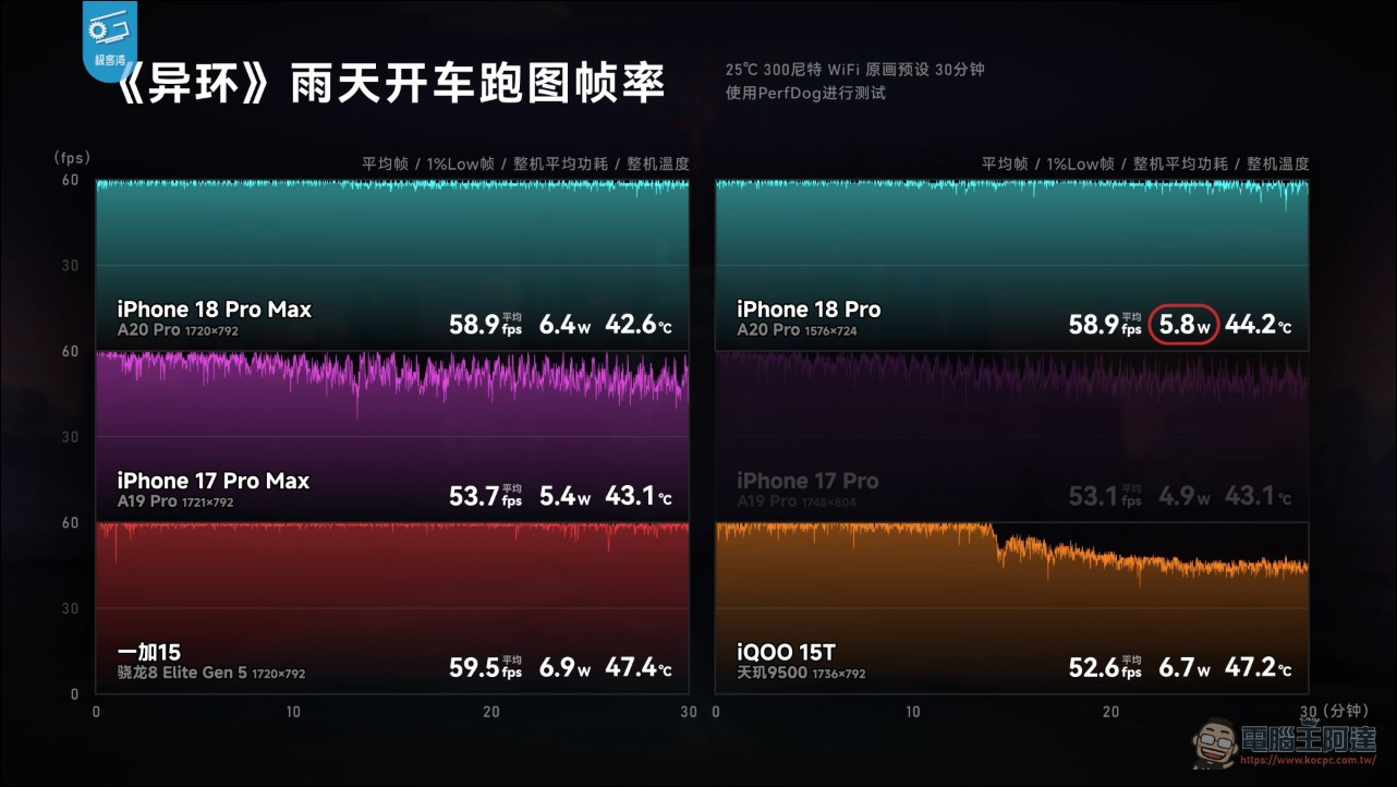
Neverness to Everness (792p) was an even tougher test: the iPhone 18 Pro Max averaged 58.9 fps, with total device power consumption of 6.4 W and a surface temperature of only 42.6°C. Geekerwan said, “I’ve never seen an iPhone sustain such high power consumption at this temperature.”
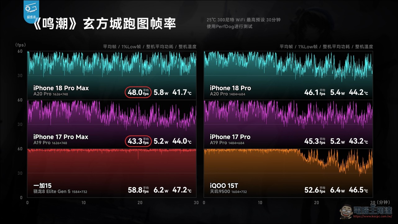
Wuthering Waves (748p) is the least iPhone-friendly, with the Pro Max only nearing 50fps and trailing the OnePlus 15, but its surface temperature stays under 42°C, a major improvement over the previous generation.
Battery life: 5,400mAh battery lasts 10 hours 37 minutes
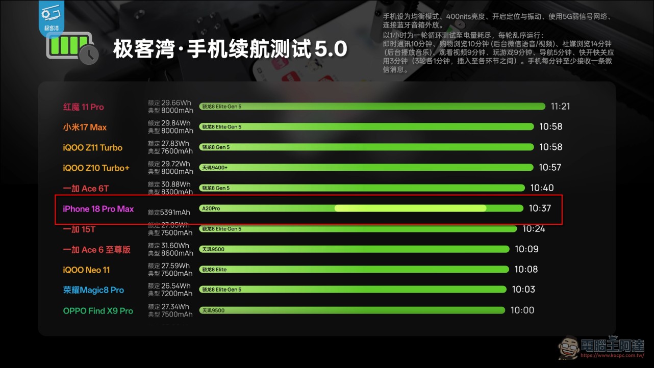
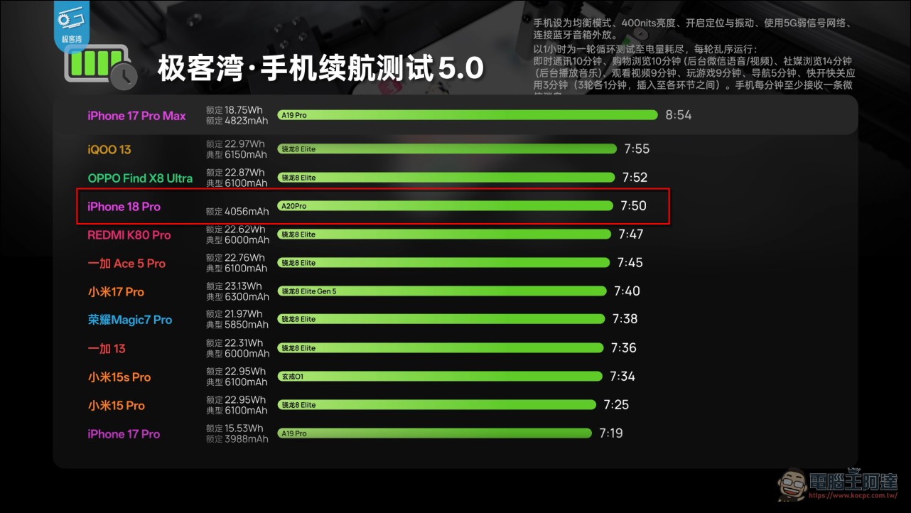
The iPhone 18 Pro Max (China model) increases its battery from 4,800mAh to nearly 5,400mAh, and with Apple’s in-house C2 baseband replacing Qualcomm’s solution, it scored 10 hours 37 minutes in Geekerwan’s 5G battery life test 5.0, nearly 2 hours more than the iPhone 17 Pro Max. The neighboring models on the chart are all 7,000-8,000mAh Android flagships. The smaller iPhone 18 Pro’s battery increases by only 100mAh, with battery life of 7 hours 50 minutes, half an hour more than the previous generation. With 5,400mAh against the 8,000mAh touted by the Android camp, the iPhone 18 Pro Max can still tie, thanks in no small part to the A20 Pro’s efficiency advantage.
However, Geekerwan also pointed out that the 18 Pro’s battery life did not live up to Apple’s launch-event claim of “surpassing the previous-generation Pro Max.”
Conclusion: The biggest chip upgrade in five years, but with two regrets.
Geekerwan concluded that the A20 Pro is the biggest chip upgrade for iPhone in five years. Against the backdrop of a marked slowdown in semiconductor process progress, Apple has delivered leapfrog improvements two years in a row, each bigger than the last. The iPhone 18 Pro series also fixes several past weaknesses at once: cooling catches up to gaming phones, battery life catches up to big-battery Android phones, and charging speed has caught up with the market pace.
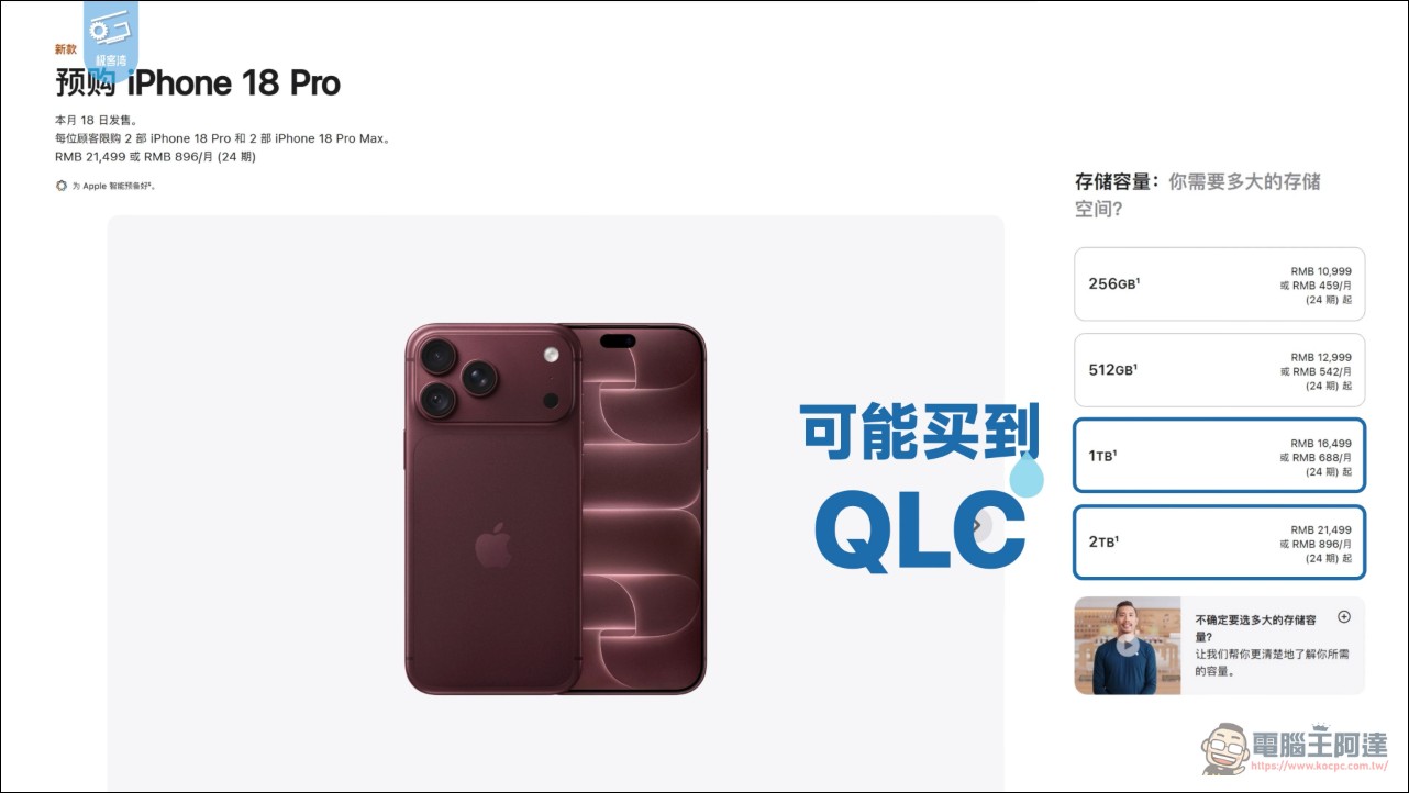
Two disappointments: first, the Pro Max weighs a hefty 250 grams, making it a true “half-jin phone”; second, the 1TB and 2TB versions are likely to use QLC flash memory, which is one of the few blemishes amid rising storage prices.
Geekerwan believes Apple’s product positioning has never been clearer: the goal of the Pro series is to become the most practical, most durable conventional flagship, eliminating all weaknesses; exploring the future form factor of phones is left to the iPhone Air and the foldable iPhone Duo. As Yunfei put it: “Apple took Android’s playbook, but ran faster than Android.”
For other details, I highly recommend everyone watch the Geekerwan video; I personally really admire that such a detailed review was produced in such a short time:
Source: KOCPC Chinese