


In 2021, during the cryptocurrency mining boom, NVIDIA launched a dedicated mining card, the CMP 170HX. This card is equipped with the exact same GA100 chip as the data center flagship A100, featuring HBM2e memory bandwidth of up to 1,500 GB/s, with a factory price of approximately US$5,000 (around NT$162,500). However, as Ethereum transitioned to a proof-of-stake mechanism, the CMP 170HX mining cards were retired within just half a year, and their second-hand prices plummeted to US$400–500 (around NT$13,000 to NT$16,250). In June 2026, Arizona State University researcher Jon Pry published a paper titled〈A Canary in the Crypto Mine: Defeating Stack Protection in a GPU Secure CoprocessorThe paper reveals a stack protection vulnerability in NVIDIA’s Falcon security co-processor. Without touching the signing keys, connecting debug interfaces, or opening the card, the research team used pure software to remove all restrictions on the CMP 170HX’s compute limits, memory locks, and PCIe bandwidth, transforming a useless card into the ultimate value-for-money AI powerhouse.
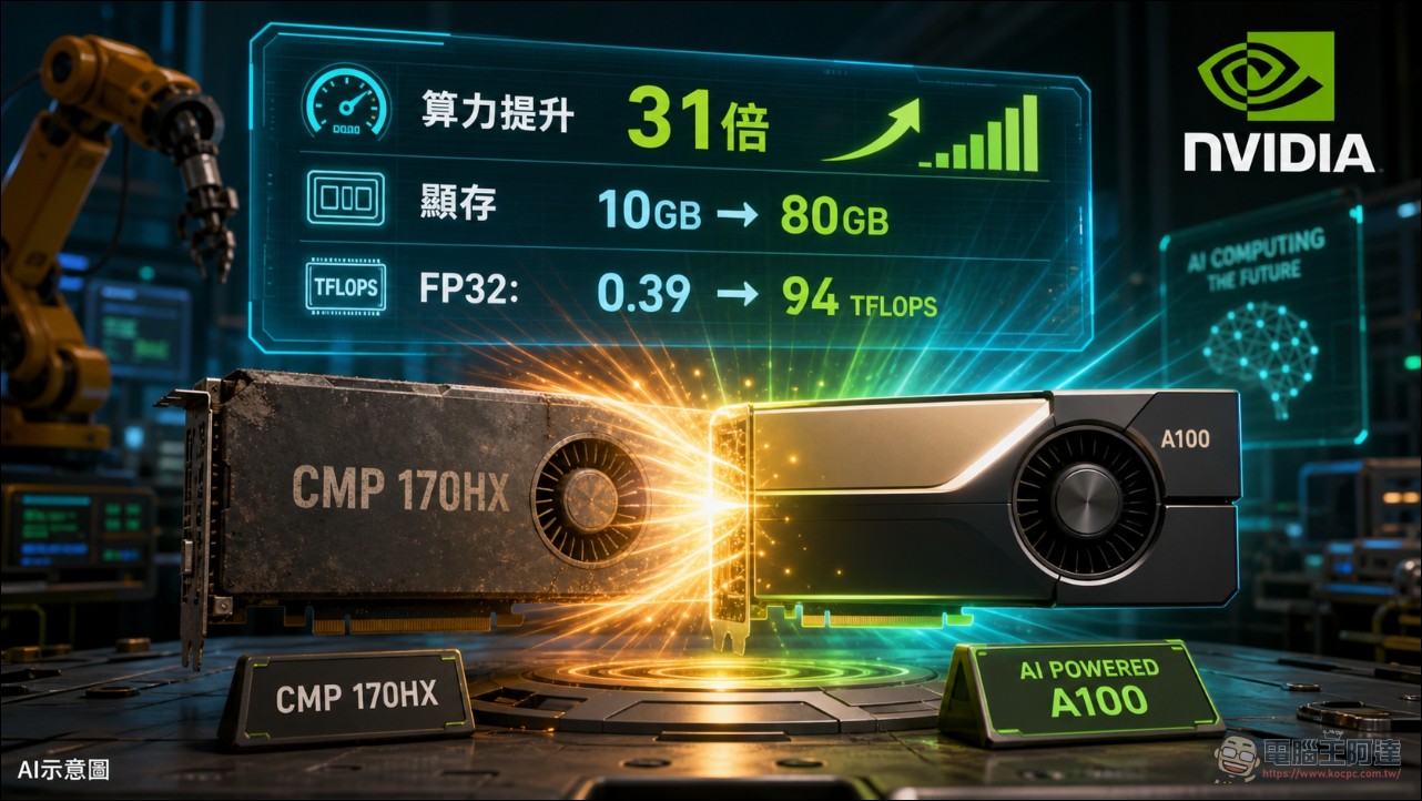
What is the CMP 170HX?
CMP 170HX is the “cut-down A100”. It uses the exact same GA100 die and HBM2e packaging, but NVIDIA applies multiple hard limits at the factory via OTP fuses (one-time programmable fuses):
- Computing power blockadeFP32 FMA/MAD throughput has been cut to only 0.39 TFLOPS, just 2% of the original A100, and even worse than GPUs from 15 years ago.
- VRAM lockAlthough the full HBM die is physically packaged, the firmware only allows access to 8GB or 10GB.
- PCIe downclockingThe original PCIe Gen4 x16 is reduced to Gen1 x1, with a bandwidth of only 1 GB/s, and the AC coupling capacitors for the 12 lanes on the PCB are simply omitted and not soldered.
- No NVLinkCompletely disable GPU interconnect functionality.
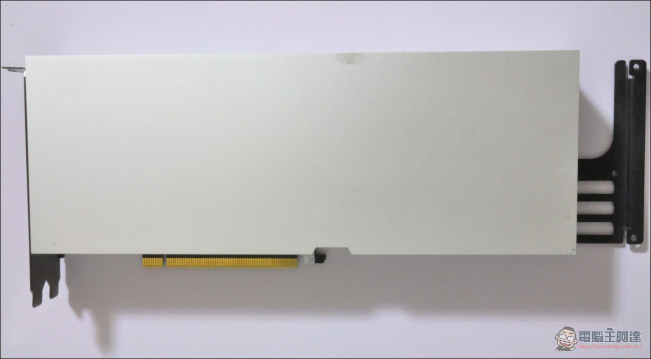
NVIDIA officially claimed that the above restrictions are permanently locked by OTP fuses and irreversible at the hardware level. However, researchers found that the problem lies in the security mechanism protecting these restrictions itself.
The Cracking Principle: The Collapse of the Three-Layer Trust Stack
NVIDIA’s GPU security architecture is divided into three layers: the bottom layer is OTP fuses, which store the results of physical fusing; the middle layer is firmware in HS (Heavy Secure) mode, running in a hardware-isolated area, responsible for reading the fuses and enforcing restrictions; the top layer is conventional memory security mechanisms such as signature verification and stack protection, used to prevent tampering with HS mode.
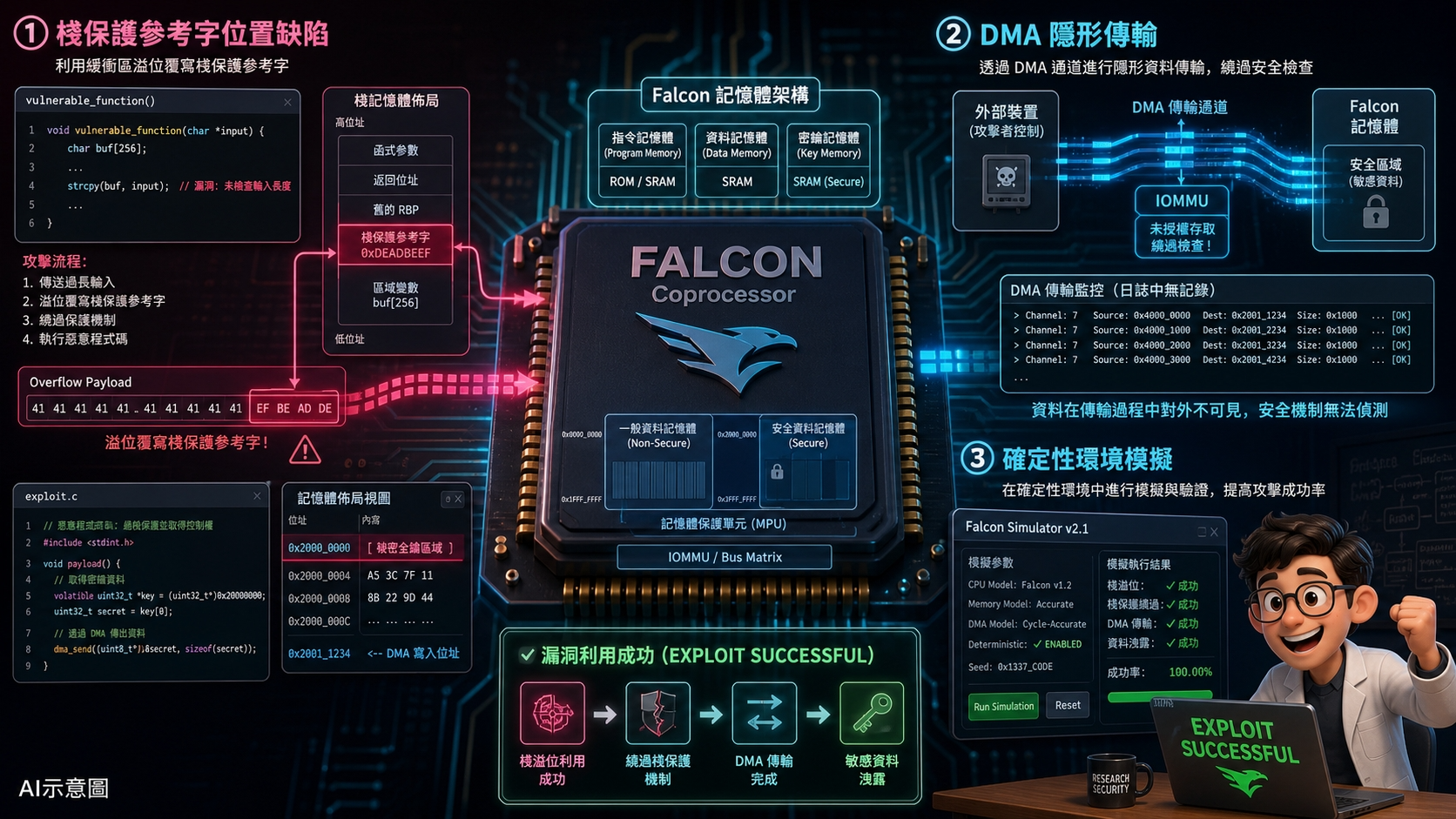
The research team directly breached the topmost layer. Once the upper layer was penetrated, the restrictions of the middle layer no longer took effect. The specific attack exploited three design flaws:
1. The stack protection reference is misplaced. The Falcon coprocessor’s toolchain defaults to __stack_chk_guard Placed at the end of the data segment, and Falcon’s data memory is flat and writable, with no MPU read-only mapping, no RELRO, no guard page. The attacker exploits a linear overflow in the signature buffer, overwriting everything with a uniform value, simultaneously covering the guard, the canary copy on the stack, and the return address—all three locations become the same value, and the check passes directly.
Second, DMA is nearly invisible in static analysis. The vulnerability entry point is an unbounded DMA copy. The LS signature verification routine pulls signature data from the host to on-chip DMEM via DMA, with the length coming from an attacker-controlled struct field, and the target buffer has no bounds checking. Conventional static analysis tools only track CPU instructions and standard library functions, and since a DMA transfer is just a few register write operations at the code level, the tools simply cannot recognize it as a memory copy.
Three, deterministic environments make offline simulation exceptionally precise. In HS mode, Falcon’s instruction memory and data memory are locked for external reads and writes, but since the microcode has no concurrency, no interrupts, and no dynamic memory allocation, the state of each cycle is deterministic. The researchers built a cycle-accurate simulator and ran the same bootloader image offline to precisely reconstruct the memory layout at the moment of overflow, without needing any real-time feedback.
Achievement Unlocked: From a Junk Card to a “Mini A100”
Using this vulnerability, the researchers loaded NVIDIA’s own signed bootloader and controlled the program counter in HS mode via unbounded DMA. After obtaining HS privileges, they rewrote the privilege level mask (PLM) to grant the host write access to the fuse override registers. They then directly modified the SM clock rate, memory configuration, and PCIe speed through PCIe BAR0.
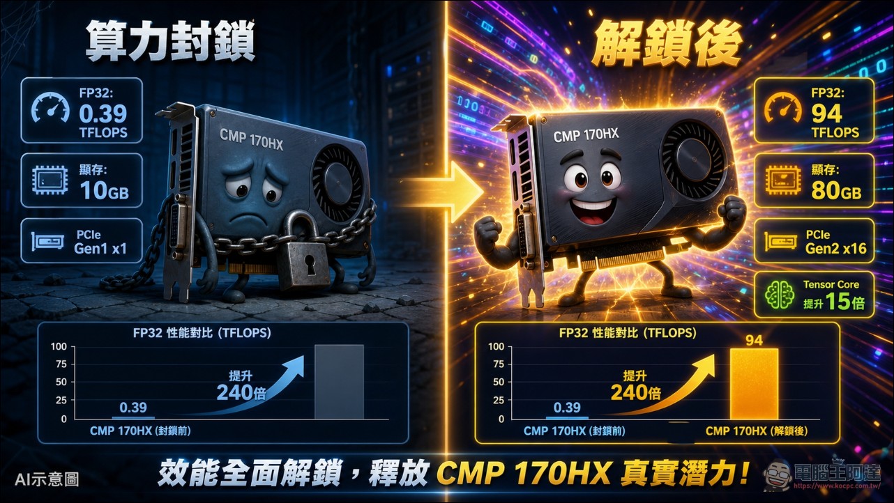
The performance improvement after unlocking is astonishing:
- FP32: From 0.39 TFLOPS to 94 TFLOPS, an increase of approximately 31 times.
- FP64Increased from 0.2 TFLOPS to 12 TFLOPS
- Tensor CoreLoad increased approximately 15 times.
- VRAMExpanding from 10GB to 80GB, writing different hashes across all addresses and reading them back for verification, confirming they are all real physical addresses.
- PCIeUpgrade from Gen1 x1 to Gen2 x16
The override value is written into the always-on power domain, and neither a functional reset nor reinstalling the driver can clear it. The entire process only needs to be performed once.
The still-unbreakable hard limit
Not all axes can be unlocked via software. PCIe Gen3 remains impossible to enable; PHY calibration parameters are suspected of being fuse-gated. The AC coupling capacitors for the 12 lanes, omitted from the PCB, must be manually soldered as 24 100nF capacitors to restore the x16 physical connection—this is a physical hard boundary. HBM mode registers and on-die ECC likewise cannot be enabled; all attempts are blocked by the source ID lock.
The paper’s author explicitly states that the status of the above limitations is “no method found” rather than “proven unbreakable,” but they at least draw a boundary line: on one side is the scope solvable by pure software, and on the other side requires at least hardware modification or deeper reverse engineering.
Practical Applications: ComfyUI and Large Language Models
After the news of the unlock spread, the Chinese community quickly began hands-on testing. Multiple Bilibili uploaders demonstrated using the unlocked CMP 170HX on Windows to run ComfyUI for AI image and video generation, and some even used it for large language model inference. Since the A100 itself supports standard NVIDIA drivers, the unlocked CMP 170HX can be directly recognized as a compute device on both Windows and Linux without requiring additional driver modifications.
The community also found that different batches of CMP 170HX use HBM memory chips from different manufacturers: the Samsung 16Gb chip version (10GB model) can be unlocked to 40GB or 80GB, while the SK Hynix chip version (8GB model) can theoretically be unlocked to 64GB. Due to the high-efficiency access characteristics of HBM’s 1024-bit bus width, data is interleaved and distributed across individual dies, and all 6 HBM stacks are physically complete and functional.
Price and purchase risk
After news of the crack spread, second-hand prices for the CMP 170HX began to rise noticeably. Currently, transaction prices on China’s second-hand market are around RMB 3,000 to 4,000 (approximately NT$13,500 to NT$18,000). In comparison, a genuine second-hand A100 40GB costs several hundred thousand NT dollars. Listings on eBay are even higher, at around US$1,500 (approximately NT$48,750).

But the risks of purchasing should not be overlooked:
- Crack stability not verifiedWith the paper published less than two months ago, there is no independent third-party testing data on long-term stability, temperature performance, or memory error rates.
- Each card has different defects.Some unlocking operations require adjustments to be made for the defective areas of individual cards; not all cards can be successfully unlocked to 80GB.
- Heat dissipation requires self-modification.The CMP 170HX was originally designed for forced-air cooling in server rooms, so most home users will need to mod it with water cooling.
- Concerns over merchant hypeSome Chinese media outlets have published articles warning that some merchants may use news of the unlock to inflate prices, while actually selling cards that are not unlocked or cannot be unlocked.
- The inherent bottleneck of PCIe Gen1Even when unlocked to Gen2, the bandwidth remains far lower than the A100’s Gen4, limiting performance in scenarios that require heavy CPU-GPU data exchange.
Safety hazard: more than just a card issue
The significance of this paper goes far beyond cracking a mining card. It reveals systemic vulnerabilities in GPU firmware security. Current AI infrastructure is driving GPU Confidential Computing, and both H100 and Blackwell support protecting model weights and inference data in multi-tenant scenarios. This approach relies heavily on HS firmware as the root of trust.
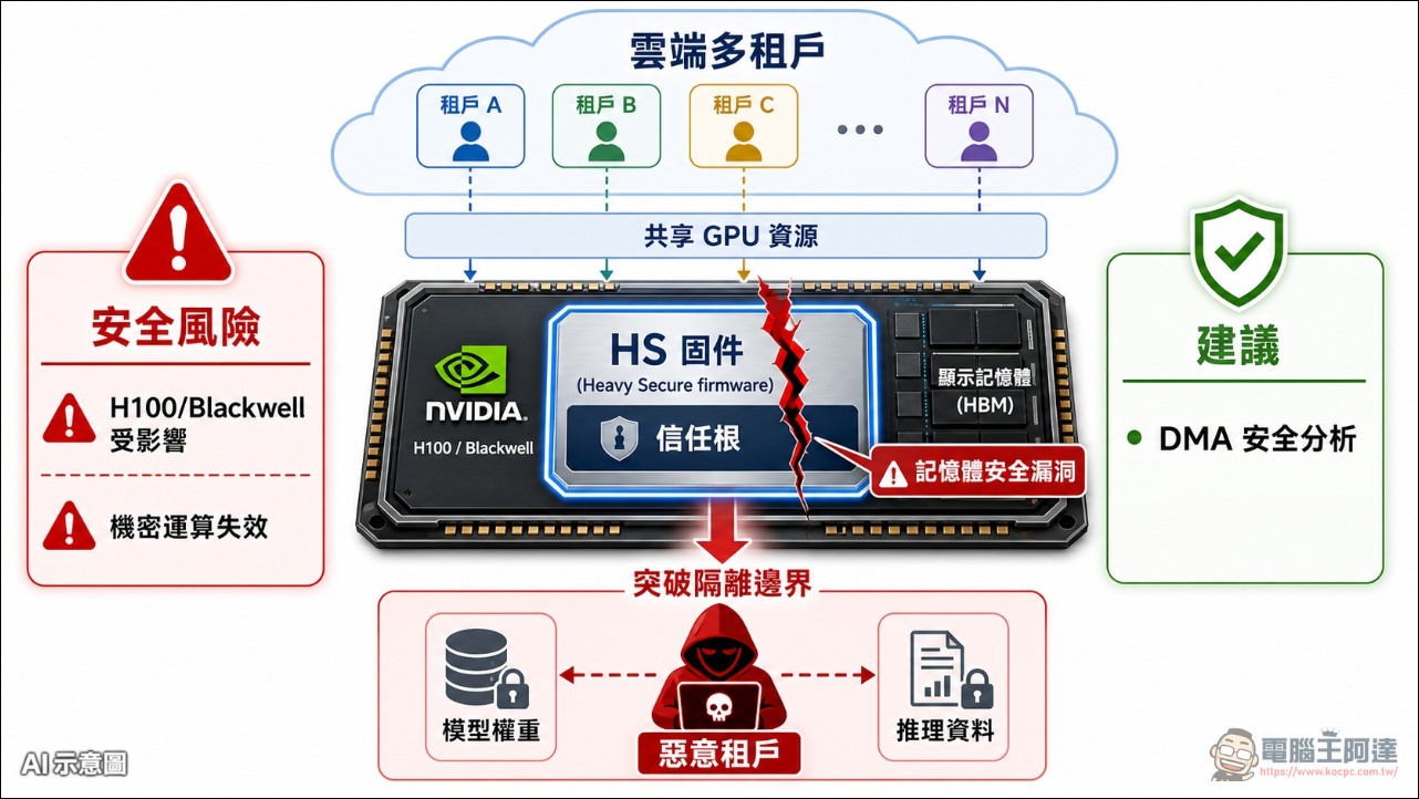
The paper directly challenges this assumption. A memory safety vulnerability — not even a zero-day — in a newly released signed bootloader could allow the host side to gain HS execution privileges. In confidential computing environments, a malicious tenant or compromised host OS could exploit this to break through the isolation boundary. The authors recommend that, when assessing multi-tenant GPU security, vendors should be required to provide DMA-aware security analysis reports.
Source: KOCPC Chinese