


Under the pressure of “American imperialism”, the Chinese began to develop semiconductor technology from scratch. Many semiconductor wafers that currently seem out of touch with the world, but can be called “advanced processes” in China, have been gradually developed. Photolithography machines, which seem unlikely to be produced in China, have also been developed, but the technology is outdated compared to the world’s mainstream technology levels. However, the old manufacturing process has to find a way to catch up. As one of the chip design companies, Huawei cannot help in this regard. It can only think of some solutions from the chip design aspect. Unexpectedly, a new Chinese technology called “wafer (chip) stacking patent” appeared in Huawei’s patent list. With this technology, even chips with backward manufacturing processes can be packed with more transistors through stacking technology, and the area can be further controlled.
Stacking semiconductor wafers sounds incredible, but it is actually a technology that major manufacturers are already trying. However, stacking two identical wafers requires a lot of complex technology, which is quite difficult to implement. Therefore, although some companies have tried to produce some, there may be many problems, so there are almost no stacked wafers that have been released so far.
Huawei’s stacked chip technology looks rich, but is it actually?
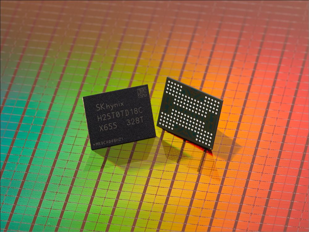
However, the concept of stacking is very practical, and memory particle technology entered the stacking stage a few years ago. By stacking tiles on top of each other, memory chips can increase their capacity, but they can be used just like ordinary chips. The current stacking world record is held by SK Hynix, which recently released new NAND Flash chips, with 321 layers. So sometimes it’s not that stacking is impossible, it’s just that different wafers or particles have different difficulties in implementation.
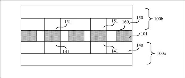
Huawei’s stacked chip patent was recently exposed. In addition to “wafer stacking structure and formation method”, there is also “wafer packaging structure”, “electronic equipment” and other contents. It seems that Huawei may not have started making its own chips, but at least it has obtained a lot of interesting things in terms of design and technology patents.
But as soon as Chinese netizens heard about the stacking technology, they thought it was a black technology of Huawei. It was all rumors about 14nm chips stacked on top of 14nm chips larger than 7nm.
According to the patent abstract, these technologies are used to simplify the fabrication process of wafer stack structures. However, simply stacking two wafers will definitely require various complex technologies, such as wiring layers, conductive structures, and how the wafers are connected and communicate with each other. As long as it works when stacked, many chips with different functions can naturally be added to make it work. If the degree of integration is high enough, the performance can increase a lot.
However, this technology is currently only a patent, and it is very difficult to implement it. Huawei needs to have a very high technical threshold to deal with various problems of stacked chips, which is much more difficult than designing a new chip. Just improving thermal management, electrical interconnection, packaging, testing and manufacturing technology is a series of extremely difficult topics.

It can be said that the principle of this technology is the same as that of stacked seat cushions, but in fact, it is not easy to operate well. Many major manufacturers, including TSMC and AMD, are working on this project. Even if Huawei has sufficient financial resources and manpower, it may be difficult to implement it. If Huawei is determined to implement this technology, it may not be possible within five or ten years.
Source: KOCPC Chinese