


A few months agoHuaweiHe Tingbo, President of the Semiconductor Business Unit, today spoke at IEEE ISCAS 2026 in Shanghai: “Tao’s lawLogical foldingway to bring semiconductor density up to the level of advanced process nodes. At the time, most media believed this might just be a concept or a technology that was all hype, but the one featured in Huawei’s recently launched tri-fold flagship Mate XT 2Kirin 9050 Pro Among the processors, the one that the Chinese tech channel Geekerwan posted at the timePerformance testingThere has already been fairly obvious progress. Recently, Geekerwan released another new video, “Deep Dive into Logic Folding! How Powerful Is the Tao Chip in Huawei’s Mate 90 Series?”, actually taking the Kirin 9050 Pro processor to the lab for cross-sectioning, reconstructing its internal structure in 3D, unraveling the mystery of the “logic folding” packaging, and then using the Mate 90 Pro Max to test gaming and battery life in real-world conditions. To get straight to the conclusion: this chip uses two dies, top and bottom, “folded” and stacked, raising transistor density by 28% without a process-node change, and its measured energy efficiency even beats Google’s Tensor G6 this year.
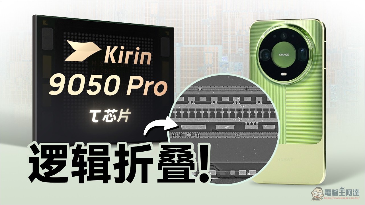
Geekerwan clip breaks down Huawei Kirin 9050 Pro logic folding technology.
Tao Chip Family: 9030, 9035, and 9050 Pro
Huawei’s Mate 90 series, announced on October 1, comprises five models in total. All ship with HarmonyOS 7 out of the box, and the chip lineup is divided into three tiers: the Mate 90 uses the Kirin 9030 (8-core, 12-thread, with overall performance up 27% over the previous generation), the Mate 90 Pro uses the Kirin 9035 (specifications close to the 9030 Pro, with adjusted peak frequency, a 20% improvement), while the Pro Max and above get the star of the show, the Kirin 9050 Pro, with overall performance up 31% over the previous generation’s flagship.
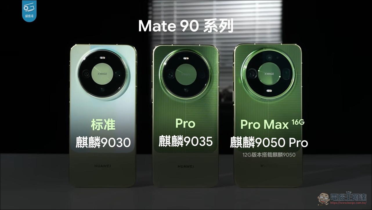
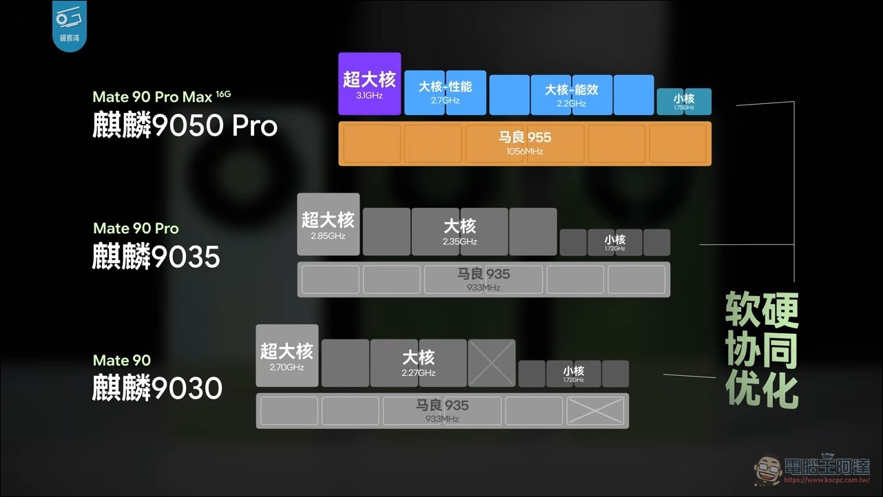
This generation of chips has a unified name, the “Tao Chip,” and behind it is Huawei’s self-developed “Tao (τ) LawUsing “time scaling” instead of traditional “geometric scaling” improves performance without relying on EUV lithography machines. The official goal is to achieve transistor density in Tao’s Law chips equivalent to that of a 1.4nm process by 2031. Both the 9030 and 9035 follow Tao’s Law but do not use logic folding; this technology is currently exclusive to the top-of-the-line 9050 Pro.
A Cutaway View: Chip Hamburger and 80,000 TSVs
After Geekerwan cross-sectioned the Kirin 9050 Pro, the structure it revealed is completely different from that of traditional chips. In an ordinary chip, metal layers are stacked layer by layer upward from the substrate, with logic circuitry buried at the top; the 9050 Pro, by contrast, has two pieces arranged face-to-face above and below, with Cu-Cu hybrid bonding in the middle bonding the metal layers together. This entire “chip burger” is then sandwiched between two layers of silicon and does not directly contact the package substrate. The top piece is the main die, built on a more advanced process; the bottom piece is the secondary die. The logic circuits in the two pieces communicate through the metal layers and the Cu-Cu bonding.
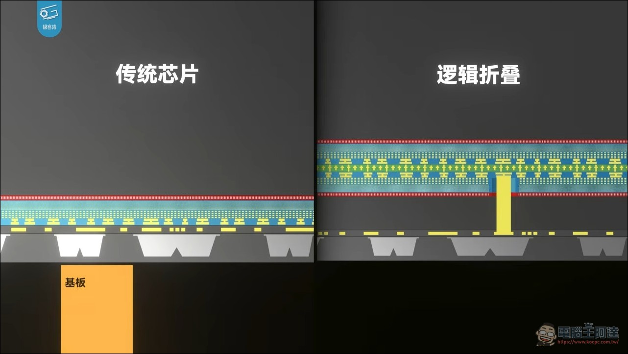
Being sandwiched between silicon creates a power-delivery challenge; the solution is TSV through-silicon vias: conductive paths pass through the underlying silicon and logic circuit area, all the way to the bonding metal layer. Geekerwan counted that HiSilicon made about 80,000 TSVs between the chip and substrate, at the cost of about 8% of the lower die’s usable area being given up to the vias and keep-out zones.
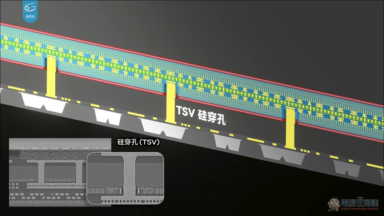
Official data also aligns with this approach: the 9050 Pro has 5 million signal transmission bonds, a cross-die transmission bandwidth of 125 TB/s, a 30% reduction in critical-path latency, a 55% reduction in buffer count, and a transistor density of 238 million per square millimeter—a 28% increase over the previous generation.
Logical folding really does fold up each core and put it away.
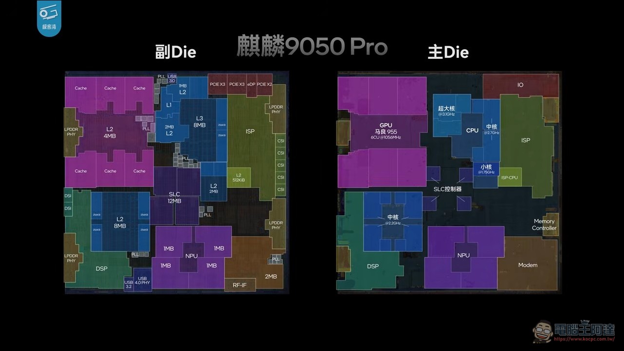
Logic folding isn’t as crude as putting the CPU on top and the GPU on the bottom. Geekerwan laid out the two dies and found that each CPU core is split into upper and lower halves: the super core’s execution units (integer, floating point, Load & Store) stay on the main die, while L1 and L2 caches go on the secondary die. After folding, the cache sits directly beneath Load & Store and is directly connected via copper bonding. Wiring distance is greatly shortened, latency drops, voltage is lower at the same frequency, and power consumption falls with it. All IP blocks on the chip follow the same strategy: cache, I/O, and PLL—parts with low thermal density and low process sensitivity—are placed on the secondary die, while high-density, high-heat compute units go on the main die.
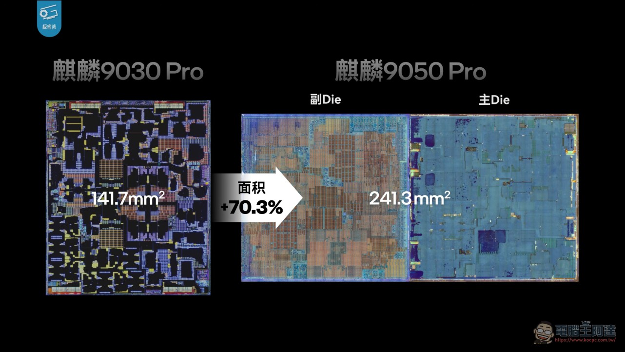
The resulting integration density is impressive: the top and bottom dies are each about 120-plus square millimeters, and the stacked footprint is smaller than the previous generation’s 140-plus square millimeters, yet the combined bare-die area of 240-plus square millimeters is a full 70% larger—equivalent to cramming 70% more circuitry in without changing the process node or increasing footprint. This is exactly the path Huawei was forced onto: since it cannot get EUV equipment and its process is stuck in place, it turned packaging and stacking into a new battleground, using 3D reconstruction to bypass the limits of planar scaling.
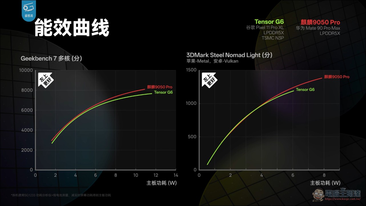
What’s more awkward is that the Kirin 9050 Pro even beats the Tensor G6 processor, which uses TSMC’s N3P 3nm process, in energy efficiency curve performance (though the Tensor series has never made high performance its main selling point, focusing instead on AI performance).
Kirin 9050 Pro Gaming and Battery Life Test
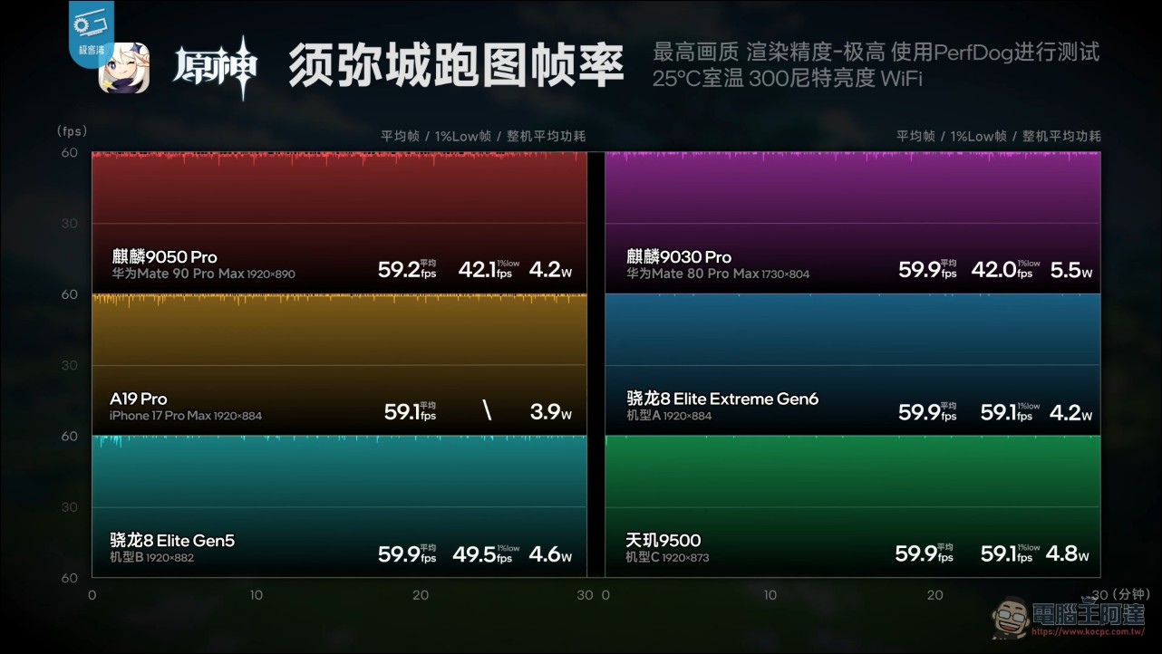
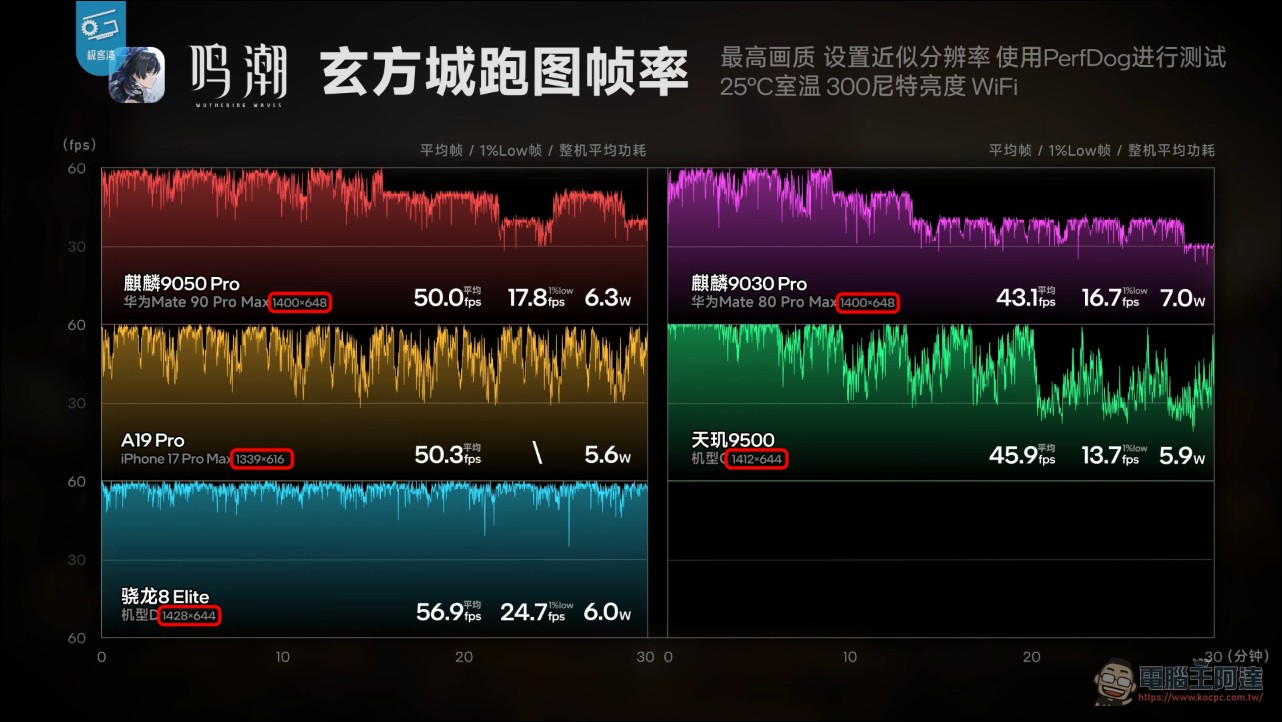
Beyond the spec sheet, the Mate 90 Pro Max also has plenty to show in real-world testing. In Genshin Impact 7.0 at 890P resolution and high-performance mode, the whole device draws just 4.2W to hit a steady 60 fps, making it more power-efficient than the previous-generation Mate 80 Pro Max at a lower resolution, and putting it not far behind Qualcomm’s latest flagship and Apple A19 Pro devices. The more demanding Wuthering Waves averaged 50 fps at 6.3W over 30 minutes of map traversal at 648P, while Ananta managed 53 fps at 6.8W, a full 10 fps more than the previous generation, with power efficiency nearly matching Android’s Dimensity 9500 and Qualcomm flagship platforms. Geekerwan also pointed out the caveat: this is treatment only HarmonyOS-native games get. Games that haven’t come to HarmonyOS have to run through a translation layer, which is smooth but not power-efficient.
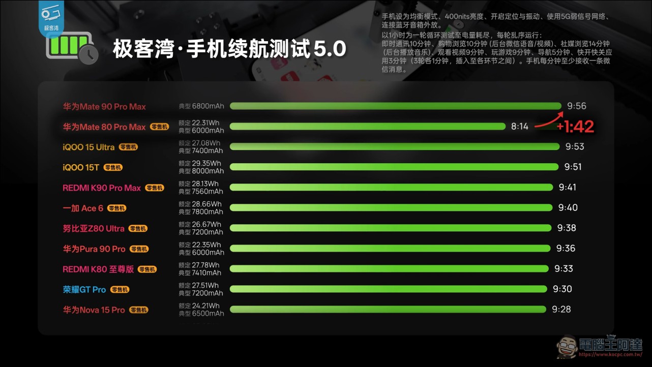
With the battery bumped up to 6,800mAh and improved chip power efficiency, it lasted 9 hours 56 minutes in Geekerwan’s 5G battery life test, more than an hour and a half longer than the previous generation, and holds its own against a bunch of big-battery Android phones.
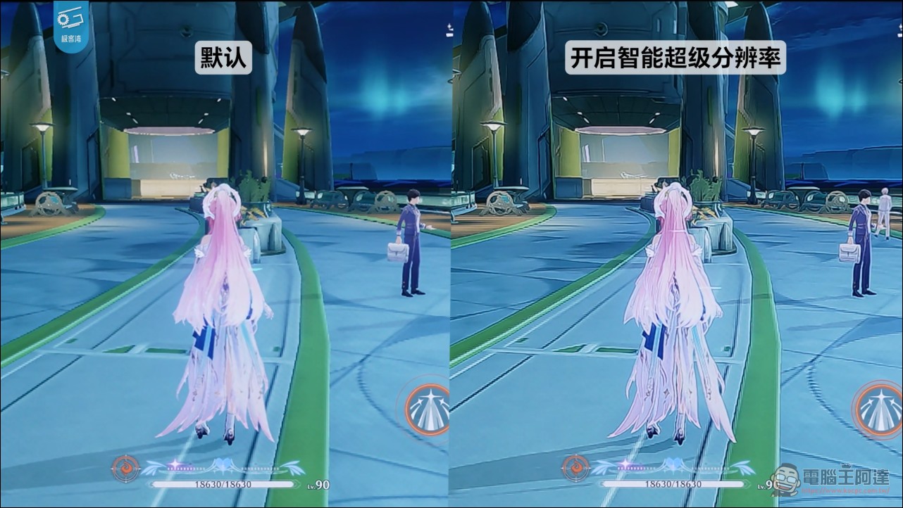
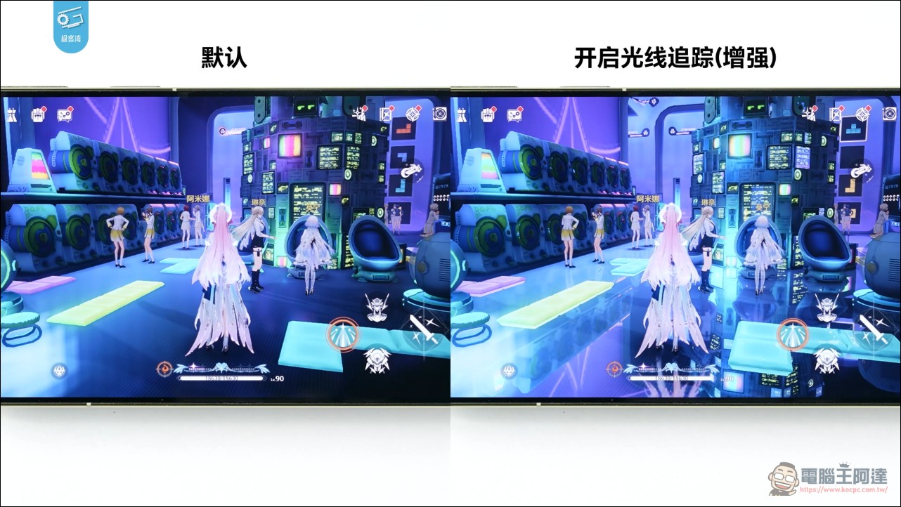
This generation of graphics technology also adds AI super resolution (with NPU and GPU working in tandem), hardware ray tracing support for more games (the ray-traced reflections in the HarmonyOS version of Wuthering Waves are visible to the naked eye), and in-game smart HDR.
NPU: 150% more area and stronger local AI capabilities
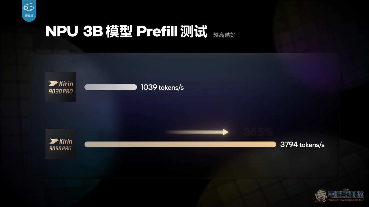
Geekerwan says this NPU is ridiculously large: the NPU area on the main die alone exceeds the entire NPU of the Kirin 9030 Pro, and the combined area of the upper and lower dies is 150% more than the previous generation. INT8 throughput is 68 TOPS, and its Prefill speed when running a 3B model is three times that of the previous generation. The official specs echo this: the Da Vinci architecture NPU improves performance by 140% and supports on-device 30B MoE large models.
In practical use, even offline, you can ask Xiaoyi to organize your photo album (running a 30B-a2B MoE model). When editing photos, the MoE model first analyzes the image and gives suggestions for removing passersby and adding blur, then hands it off to a local 6B multimodal model to do the actual editing, and the results are no worse than cloud models. If you want to learn more about the capabilities of the Kirin 9050 Pro, you can also watch Geekerwan’s video directly. Personally, I’m also very impressed by the performance of Huawei’s processor this time.
Conclusion: The Third Path Folded Out
Geekerwan spoke highly of logic folding, but also pumped the brakes: the technology is currently expensive, yields are still ramping up, and in the short term it will only be used in flagship products. Huawei itself defines Tao’s Law and logic folding as an inclusion relationship, and not every chip will fold. The price says it all: the 16GB + 512GB version of the Mate 90 Pro Max sells for RMB 9,999, about NT$44,000, which is RMB 2,000 more than the same configuration of the previous generation. Yu Chengdong admitted that rising memory prices add an average of US$200 to the cost of each phone. For the semiconductor industry, logic folding offers an intriguing demonstration: as the door to process scaling gradually narrows, packaging, stacking, and architectural design—these “back-end efforts”—can likewise push chips forward a generation. Whether this path can go far will ultimately test yields and the cost curve.
Source: KOCPC Chinese