


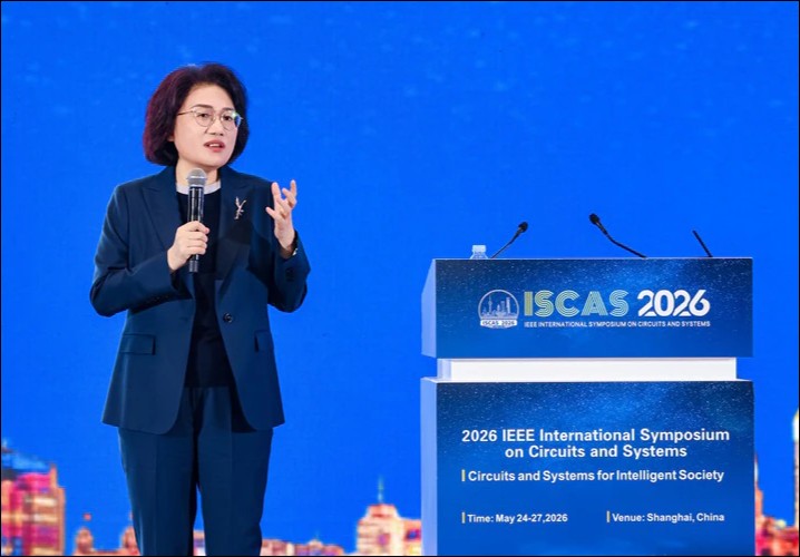
He Tingbo, President of Huawei’s Semiconductor Business Unit, announced “Tao’s Law” at IEEE ISCAS 2026 in Shanghai today, a new semiconductor development path that replaces geometric shrinkage with time shrinkage. Through LogicFolding logic folding technology, Huawei aims to achieve an “equivalent” transistor density of 1.4nm in 2031, directly bypassing the dependence on ASML High-NA EUV lithography equipment.
Huawei publishes “Tao’s Law” to combat Moore’s Law
As Moore’s Law approaches the physical limit, the size of transistors has approached the atomic scale, and the quantum tunneling effect and leakage current have exponentially increased the cost of each generation of process shrinkage. The entire semiconductor industry is looking for the next way out. TSMC, Intel, and Samsung are still moving forward along the path of geometric shrinkage, but the development time and capital expenditure of each generation of nodes are constantly lengthening.
Huawei gave a different answer today.
At the 2026 IEEE International Symposium on Circuits and Systems (ISCAS 2026), He Tingbo, director of Huawei and president of the Semiconductor Business Department, delivered a keynote speech titled “Exploration and Practice of New Paths for Semiconductors” and formally proposed the “Tau Scaling Law”. This new law, named after the Greek letter τ (tau, which stands for time constant), advocates using “time micronization” to replace the “geometric micronization” that has dominated industrial development in the past few decades.
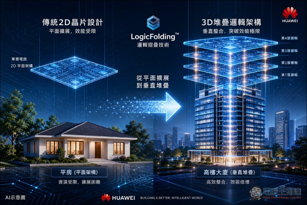
In his speech, He Tingbo used a simple metaphor to illustrate the difference between the two: traditional Moore’s Law is like building a bungalow, by making the bricks (transistors) smaller and smaller, and packing more transistors into the same area; Tao’s Law is transforming a bungalow into a high-rise building, using Logic Folding technology to move circuits from a single-layer plane to a multi-layer three-dimensional structure.
The core of Tao’s law: τ = R × C
The mathematical basis of Tao’s law is extremely simple: the time constant τ is equal to the circuit resistance R times the parasitic capacitance C (τ = R × C), which represents the delay time for the signal to propagate in the circuit. The new direction proposed by He Tingbo is: instead of continuously shrinking the physical size of the transistor, it is better to systematically reduce the τ value to make the signal run faster, rather than making the transistor smaller.
To this end, Huawei has constructed a “multi-level collaborative optimization system” covering four levels:
- device level: Optimize the transistor, interconnection resistance and parasitic capacitance, and minimize the device-level τ value from the physical bottom layer
- circuit level: Breaking through the physical boundaries of traditional plane layout through LogicFolding technology, significantly shortening the winding length of critical paths, and effectively reducing the resistance and capacitive load of signal propagation
- chip level: Improve system-level parallelism and efficiency through full-stack software and hard-core co-design of “software, architecture, and chips”
- system level: Define the Lingqu bus, reconstruct the computing system interconnection protocol, and significantly reduce the system communication delay.
LogicFolding: Transforming chips from bungalows to buildings
LogicFolding is the core implementation technology of Tao’s Law. In traditional chip design, logic units are arranged in a planar manner on the surface of the chip, and all signals are transmitted in two-dimensional space. As process nodes advance, wiring delay has exceeded transistor switching delay and has become the main bottleneck for performance improvement.
Huawei’s LogicFolding technology transforms logic circuits from two-dimensional planes to three-dimensional stacks. He Tingbo revealed that the “Kirin 2026” mobile phone chip, which will be released in the autumn of 2026, will expand from single-layer logic design to double-layer logic folding, which is the first successful commercial implementation of Logic Folding technology. This is also a key step for Huawei to break through the “saturation zone” of chip performance for the first time since the launch of Kirin 9030 Pro in 2025.
He Tingbo revealed an important quantitative data in his speech: In the past six years, Huawei has designed and mass-produced products based on Tao’s Law. 381 types of chips, covering multiple fields such as communications, computing, and terminals. This number not only demonstrates Huawei’s ability to continue to produce chips despite U.S. sanctions, but also provides practical verification of the feasibility of Tao’s Law for large-scale mass production. These chips cover the complete evolution path from early exploration to mature application, which illustrates from the side that this technical route is not just a talk on paper, but has been gradually implemented in actual products.
The race with TSMC: Targeting 1.4nm equivalent process in 2031
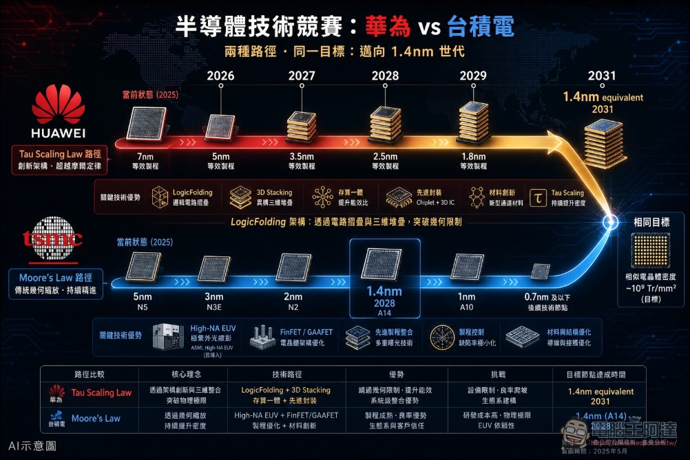
According to Huawei’s technology roadmap, high-end chips based on Tao’s Law are expected to Achieve transistor density equivalent to 1.4nm process in 2031. For comparison, TSMC’s A14 (1.4nm) process is expected to 2028 Entering mass production, it adopts the second-generation GAAFET (gate surround transistor) architecture and needs to be equipped with ASML’s High-NA EUV lithography equipment. In other words, Huawei aims to narrow the current process gap of about five years to about three years. Even more revolutionary, this goal is to Completely independent of ASML High-NA EUV devices proposed under the premise.
Since 2020, the United States has implemented multiple rounds of semiconductor export controls on Huawei, restricting Huawei’s access to advanced process equipment and EDA tools. One of the most destructive measures is to ban ASML from shipping EUV and High-NA EUV lithography equipment to China. Traditionally, advanced processes below 5nm are highly dependent on such equipment.
This is the core strategic significance of Tao’s Law and Logic Folding: it bypasses the dependence on extreme process equipment from the design methodology level. By achieving higher transistor density and performance on more mature processes through circuit architecture innovation, Huawei and its manufacturing partner Semiconductor Manufacturing International Corporation (SMIC) can continue to catch up with the performance levels of advanced processes without acquiring High-NA EUV equipment.
Market reaction: Chinese semiconductor stocks surge
After the news was announced, Chinese semiconductor stocks surged across the board. The Shanghai Science and Technology Innovation Board chip index soared 4.81%, with Cambrian rising more than 11%, SMIC rising 5.47% to 6.46%, and Huahong soaring 16.45% to a record high. Semiconductor ETFs have also attracted significant inflows.
However, although Tao’s Law provides a new path to bypass advanced manufacturing processes, it still faces many technical challenges. Thermal management is the first problem. Vertically stacking logic cells will increase power density and heat dissipation requirements will increase significantly. The second is interconnection complexity. Multi-layer folding requires more complex winding and routing designs. In addition, whether the EDA tool ecosystem can support such three-dimensional logic design and the impact of multi-layer folding on yield are all problems that need to be gradually overcome.
summary
From a more macro perspective, the release of Tao’s Law marks an important industry milestone. He Tingbo emphasized at the end of his speech: “The future must be one of open cooperation. Under the path of Tao’s Law, we look forward to working closely with global scientists, engineers, and industry partners to jointly promote the sustainable development of the semiconductor and electronics industry.” These words show that after Huawei has completed its independent technological breakthroughs, it intends to promote Tao’s Law as a new path for the global industry to follow.
There are still five years to go until 2031. It will take time to verify whether Tao’s Law can really lead Huawei to bypass ASML’s EUV blockade and narrow the gap with TSMC. But what is certain is that at the crossroads where the semiconductor industry is looking for the direction of the post-Moore era, Huawei has given a Chinese-style answer, and this answer is attracting global attention.
Source: KOCPC Chinese